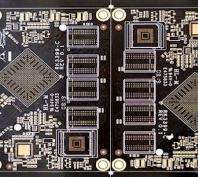
High-frequency circuit wiring skills in PCB design
To ensure high-quality signal transmission and reliability in high-frequency PCB designs, adhering to effective wiring strategies is essential. Here are optimized guidelines and techniques, with key points highlighted for easy reference:
1. Minimize Interlayer Transitions
Reducing the use of vias minimizes the interlayer transition effects and the distributed capacitance (about 0.5pF per via), improving speed and reducing data errors.
2. Shorten Lead Lengths
The signal radiation is proportional to lead length, so minimize distances in high-frequency signal paths, especially for sensitive lines like clocks, crystal oscillators, DDR data, LVDS, USB, and HDMI lines.
3. Reduce Bends in Leads
Prefer straight lines for high-frequency leads. If bending is necessary, use 45-degree or arc bends to minimize high-frequency emissions and coupling, unlike in low-frequency circuits, where this primarily strengthens copper adhesion.

4. Manage Crosstalk
High-frequency signals can induce “crosstalk” when routed closely in parallel. To reduce this:
- Insert ground wires or planes between adjacent lines.
- Avoid long parallel runs; keep critical signal lines perpendicular to nearby traces.
- Place ground planes on the reverse side of critical signal lines for better isolation.
- Use differential signaling and ground wrapping for clock lines.
- Ground any unused input terminals to avoid them acting as antennas.
5. Separate Digital and Analog Grounds
Isolate digital and analog ground planes to prevent harmonics from high-frequency digital signals from affecting analog signals. Connect them at a single point using a high-frequency choke bead or at an appropriate single location.
6. Add High-Frequency Decoupling Capacitors
High-frequency decoupling capacitors at IC power pins suppress high-frequency interference on power pins, ensuring cleaner power delivery to the ICs.
7. Avoid Loops in Routing
Loops in high-frequency traces can generate unwanted interference. If unavoidable, minimize loop area.
8. Ensure Impedance Matching
Impedance mismatches cause signal reflections, leading to overshooting and signal degradation. Match transmission line impedance with load impedance, and avoid sudden changes in trace width or bends. Specific guidelines include:
- LVDS: 7 mil line width, 6 mil spacing for differential pairs to maintain 100Ω ±15% impedance.
- USB: 10 mil line width, 6 mil spacing, with 6 mil ground-to-signal spacing.
- HDMI: 10 mil line width, 6 mil spacing for differential pairs; maintain 20 mil spacing between pairs.
- DDR: For DDR1, ensure uniform line width, equal spacing, and follow the 2W rule to prevent crosstalk. For DDR2 and higher, equalize line lengths for consistent impedance and signal integrity.
Applying these practices strengthens signal integrity and reduces interference, enhancing the overall reliability of high-frequency PCBs.
KKPCB conducts research on special processing technologies such as ordinary double-sided boards, thick copper circuit boards, high-frequency circuit boards, HDI circuit boards, rigid-flexible circuit boards, FPC flexible boards, buried blind hole circuit boards, and IC carrier boards. Provides PCB design, PCB layout, PCB prototyping and PCB assembly services.


