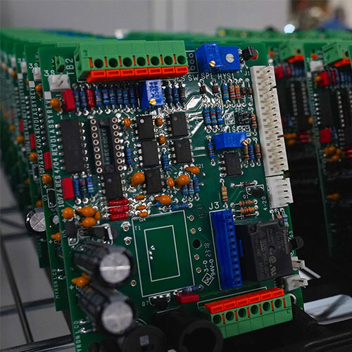
Types and Applications of Special PCBs
After years of development, CB has evolved from a general circuit board for placing components to a circuit board with complex components.
As a PCB designer or manufacturer, you are constantly challenged with how to achieve better results. You want to provide new solutions or breakthroughs to problems. In some cases, these problems may require new features. It can also be a choice between module-based or custom PCB design. In any of these cases, you need a special PCB type. The growing demand for electronic functions such as high speed or high power in odd spaces makes special circuit board types essential.
What is a special PCB?
Multilayer High Glass Transition Temperature (TG) Printed Circuit Board Manufacturer
If PCBs are classified according to materials, special PCBs can be FR4 PCBs or metal core PCBs. Special PCBs have special requirements. That’s why they are called special PCBs. For example, special PCBs such as buried blind boards, 10 ounce thick copper, and high-frequency boards have special requirements.
Specialized PCBs can achieve electrical and mechanical functions. In addition, extreme factors such as copper thickness, precision, and PCB thickness have also become the focus of attention.
Special PCB Types
Ceramic PCB: This printed circuit board has high-reliable electronic capacity, excellent high voltage, high frequency, and high insulation.
High-frequency RF board: High-frequency RF PCB uses high-frequency materials such as Taconic, Rogers, etc. The frequency range of this material is between 300MHz~3GHz.
Impedance Controlled PCB: This circuit board has two impedances of 100 ohms and 50 ohms. The tolerance is +-10%.
Thick Copper PCB: The copper weight of thick copper boards is 4~10 OZ/ft2, and the copper weight of ultra-thick copper PCBs is 20~200 OZ/ft2.
Carbon Ink PCB: If the resistance of a carbon ink PCB is 500 ohms or 100 ohms, it means that its resistance is normal. The resistance may be as high as 10,000 ohms.
How to Optimize the Specialty PCB Board Manufacturing Process
The material used for a printed circuit board mainly determines its performance. Therefore, it is crucial to choose the best PCB material. The choice of PCB material is one aspect of PCB design. However, if the PCB board material does not meet the board requirements, the PCB designer needs to explore the performance of the board.
In addition, there are also some parameters that the CM must consider during the manufacturing process of special PCBs. These parameters include material type, light copper weight, trace width, size, heavy copper weight, surface finish, etc. These parameters affect the cost and turnaround time of the manufacturing process.
As a PCB designer or manufacturer, you are constantly challenged on how to achieve better results. You want to provide new solutions or breakthroughs to problems. In some cases, these problems may require new features. It is also possible to choose between module-based or customized PCB design. In any of these cases, you need a special PCB type.
Special PCB Technology
HDI Blind Buried Via
You can only see blind vias on the top or bottom layers. This means that blind vias are usually created from the surface of the PCB. On the other hand, buried vias have both sides within the PCB layer. Buried vias are usually drilled in the inner layer. This means that a buried via is a type of hole inside the circuit board. Blind buried vias help reduce the quality and size of high-density interconnect (HDI) PCBs. In addition, these holes help enhance electromagnetic compatibility, minimize the number of layers, speed up PCB design, and reduce costs.
The integration of blind buried vias in FR-4 prototype boards has developed to a maximum of 20 layers, with a board thickness of ≤6.0mm, a blind via level of 1~4, and integrated laser drilling technology.
Multi-layer special stacking structure
As the demand for high-speed circuits continues to grow, the complexity of PCB boards has also increased, and the power layer needs to be separated from the signal layer to prevent interference from electrical factors, so this process involves multiple layers.
In addition, the stacking structure plays an important role in the electromagnetic compatibility (EMC) performance of the circuit board and is also an important way to reduce electromagnetic interference. For the number of signal networks, if the device density is greater, the PIN density will also be greater. In this case, a special stacking structure is required.
Impedance Control
Characteristic impedance refers to the resistance encountered by electromagnetic waves or high-frequency signals when components transmit signal lines. When the circuit board transmits digital signals, the characteristic impedance value of the PCB must correspond to the electronic impedance of the tail components.
In the case of mismatch, the transmitted signal energy will be reflected, delayed, attenuated and scattered. In this case, PCB designers must perform impedance control. For FR-4, flexible circuit boards, rigid-flex boards, the impedance control process can help achieve 2–20 layers.
Thick Copper PCB
Thick copper PCB is a printed circuit board with a copper thickness of 2 ounces or more. In addition, thick copper circuit boards are corrosion-resistant, low-temperature-resistant, high-temperature-resistant, and have good ductility. These characteristics make the service life of electronic devices longer. In addition, they also help to simplify the size of electronic devices. Some PCB designers can achieve 2~6 layers in thick copper PCB technology. 10 ounces is the maximum copper thickness.
Chemical Nickel Electroless Palladium Immersion Gold (ENEPIG)
Chemical Nickel Electroless Palladium Immersion Gold (ENEPIG) is a commonly used surface treatment type in circuit boards. The ENEPIG process involves chemically depositing nickel, palladium, and gold on the surface of the PCB. This surface treatment technology is non-selective.
This surface treatment option integrates a 50 nm thick palladium plating layer and a 10 nm thick gold plating layer. The integration of these plating layers helps achieve anti-friction, corrosion resistance, and good conductivity. The thickness of the copper layer affects the above different appearances and physical properties. ENEPIG is the latest surface treatment technology integrated in PCB prototypes. Plated pads
Electroplated nickel gold/gold fingers
Nickel electroplating is also called electrolytic gold. This surface treatment method integrates gold particles with electroplating, which is usually called hard gold because of its strong adhesion. This gold particle attachment process can improve the wear resistance and hardness of the circuit board, and prevent the diffusion of metals such as copper, while meeting the requirements of brazing and hot pressing welding. The plating can have good ductility, low stress, and low porosity, so the plating is widely integrated in PCB prototyping.
Considerations When Choosing a Special PCB Manufacturer
There are several special PCB manufacturers. It is vital to consider some factors when choosing a manufacturer for your special circuit board.
Expertise
Special PCBs, such as thick copper boards, ceramic PCBs, and high-frequency boards, require a lot of skills and knowledge in the manufacturing process. Your manufacturer must have a good knowledge of the design and production of such PCBs. Also, you can get more information from customer reviews.
Certification
Your special PCB manufacturer must adhere to certain standards in the industry. Also, make sure that the company you hire has the right certifications. Certification means that your PCB manufacturer adheres to certain standards in the industry. Also, it indicates the quality of the printed circuit boards provided by your manufacturer. The right certification ensures that your manufacturer is on the right track.
Experience
This is another factor that you need to consider when choosing a manufacturer for your special PCB project. Some manufacturers have long-term experience in manufacturing special PCBs. The years of experience gained by your PCB manufacturer indicate how well they perform.
Turnaround Time
The turnaround time is an important factor to consider when choosing a special PCB manufacturer. This factor describes the time it takes to complete the manufacturing of your printed circuit board. Before requesting a circuit board, ask the manufacturer about its turnaround time.
Customer Support
This is an important factor you need to consider when choosing a manufacturer for your special PCB. Your manufacturer should pay attention to all your needs and details. In addition, some PCB manufacturers also provide after-sales services to their customers. Consider a manufacturer that puts your interests first.
KKPCB conducts research on special processing technologies such as ordinary double-sided boards, thick copper circuit boards, high-frequency circuit boards, HDI circuit boards, rigid-flexible circuit boards, FPC flexible boards, buried blind hole circuit boards, and IC carrier boards. Provides PCB design, PCB layout, PCB prototyping and PCB assembly services.

