What is the Flexible PCB Manufacturing Process?
Flexible printed circuit boards (FPCBs) are essential components in modern electronic devices, offering versatility, lightweight design, and the ability to adapt to a variety of shapes. The manufacturing process of flexible PCBs involves several key steps, each of which is critical to ensuring the quality and performance of the final product. This article outlines the main stages of FPCB manufacturing, including design, material selection, processing, and finishing.
- Design and Engineering
The manufacturing process begins with the design phase, where engineers use specialized software to create the layout of the flexible PCB. This involves defining circuit traces, pads, vias, and other basic features. Key considerations at this stage include:
– Electrical requirements: Ensure that the design meets the electrical specifications and functionality required for the intended application.
– Mechanical constraints: Consider flexibility, bend radius, and space constraints within the device.
– Thermal management: Consider heat dissipation requirements based on the operating environment.
Once the design is complete, a Gerber file is generated that serves as a blueprint for the manufacturing process.
- PCB Material Selection
Choosing the right material is critical to the performance of the FPCB. Common materials include:
– Substrate: Flexible substrates are typically made of polyimide or polyester. Polyimide is favored for its high temperature resistance and excellent electrical properties. –
Conductive material: Copper is the most commonly used conductive material, chosen for its high conductivity and reliability. –
Adhesive: Used to bond the layers and ensure mechanical stability. Options include pressure-sensitive adhesives and thermosetting adhesives.
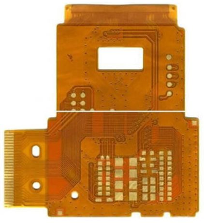
The selected material must meet the intended use, ensuring durability, flexibility, and performance.
- PCB Printing and Etching
Once the material has been selected, the next step is to create the conductive traces on the flexible substrate. This involves several sub-processes:
– Copper coating: The flexible substrate is first covered with a thin layer of copper as the conductive material.
– Photoresist application: A layer of photoresist film is applied to the copper surface. This film will determine the areas where the copper will remain after etching.
– Exposure and development: The board is exposed to ultraviolet (UV) light through a photomask that outlines the desired circuit pattern. The exposed areas of the photoresist dissolve and are washed away, revealing the copper underneath.
– Etching: The board is then placed in an etching solution, usually ferric chloride or ammonium persulfate, which removes the unprotected copper, leaving behind the desired circuit traces.
Flexible Circuit Boards
- Layer Stacking (for Multilayer FPCBs)
For multilayer flexible PCBs, additional layers must be bonded together. This involves:
– Layer Alignment: Carefully aligning each layer to ensure that the circuit paths are properly connected.
– Bonding: Bonding the layers using adhesives or lamination processes. Heat and pressure may be applied to ensure a strong bond.
– Drilling: Vias are created using laser drilling or mechanical drilling to establish connections between layers. Laser drilling is favored for its high precision and ability to create smaller vias.
- PCB Surface Treatment
Surface treatment is required to protect the copper traces and improve solderability. Common methods include:
– ENIG (Electroless Nickel Immersion Gold): Provides excellent solderability and corrosion resistance.
– OSP (Organic Solderability Preservative): A cost-effective option that protects copper without the use of metal.
– HASL (Hot Air Solder Leveling): Coats a layer of solder over the copper, providing a surface that can be directly soldered.
Each finishing method has its advantages and can be selected based on the specific requirements of the application.
- PCB Testing and Quality Control
Quality control is critical in flexible PCB manufacturing. Several tests are required to ensure that the board meets the required specifications:
– Visual Inspection: Thoroughly inspects for defects such as scratches, misalignment, or incomplete etching.
– Electrical Testing: Automated Test Equipment (ATE) checks the circuit for continuity and shorts.
– Mechanical Testing: Bend and flex testing ensures that the PCB can withstand the stress of its intended application.
In addition, companies can employ Statistical Process Control (SPC) techniques to continuously monitor and improve the manufacturing process.
- PCB Cutting and Finishing
After successful testing, the FPCB is cut to final size. This may involve:
– Die Cutting: A method that uses a die to punch out the desired shape from the flexible material.
– Laser Cutting: Provides high precision and can accommodate complex designs.
After cutting, the edges may be processed to remove burrs and ensure a smooth surface.
- Final Inspection and Packaging
Before shipping, a final inspection is performed to verify that all specifications are met. This may include checking the appearance, size, and functionality of the FPCB. Once inspected, the boards are carefully packaged to prevent damage during shipping.
The manufacturing process for flexible PCBs is complex and requires precise control of each step to ensure high-quality results. As technology and materials advance, the capabilities of FPCBs continue to expand, enabling more complex and compact designs in a wide range of applications, from consumer electronics to medical devices. Understanding this process is critical for engineers and manufacturers aiming to optimize flexible PCB production to meet their specific needs.

