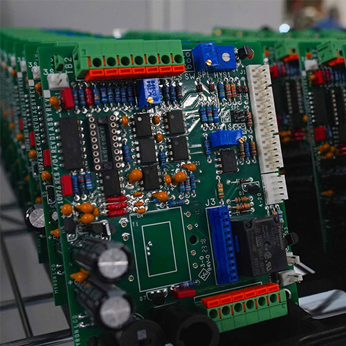
What is Backdrill and How Was It Done in PCB Manufacturing?
What is Backdrill?
Back drilling is a method to remove the via stub from the specific layer of multilayer PCB. Via stub is a non-functional portion of a plated through hole or via barrel which can cause unwanted reflection leading to signal distortion and lower performance. It is recommended that the diameter of the back drill hole be greater than that of the via hole size.
Below is a diagrammatic description of back drilling:
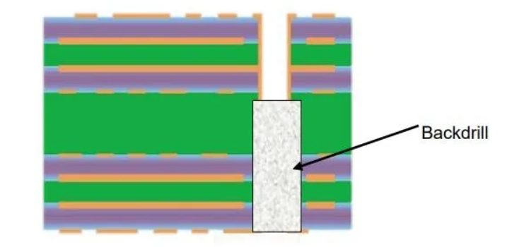
To understand the process Let’s take the example, of a 12-layer PCB, High-speed signals are running between layers 1-8. The via hole passes through the layer 1 to 12. But vias have electrically connected only layer 1-8 and there is unnecessary vias plated 9-12. In this case, we can remove via stubs that are not electrically connected on layers 9-12.
Why Use Backdrill in PCB Manufacturing?
When we input the original signal, the input signal will be interfered with by noise causing signal loss and adverse effects, which is why we need it in the manufacturing process. To remove this unwanted loss and improve the signal integrity we can use the back drilling process. It minimizes the signal reflection and alternating improves signal quality. This is also referred to as a Controlled depth drill (CDD). Signal Integrity matters in the high-speed PCB design.
If the design contains a high-speed communication system or sensitive analogue circuit, back drilling is a good technique to meet the performance requirement.
The Advantages of Backdrill are:
- Reduced unnecessary signal loss.
- Reduce the error bit rate
- Lower cost than sequential lamination.
Back drilling in HDI PCBs is preferable to blind vias drilling as it requires a special laminate stack-up. Backdrill hole quantity should be limited otherwise more quantity of back drill adds more costs.
How was Backdrill Done in PCB Manufacturing?
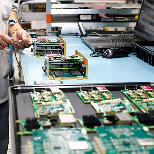
This process involves using a special CNC machine to drill the via stub from the opposite side of the board. The diameter of the back drill should be slightly larger than the diameter of the via. Typically, backdrills are 6-8mil larger than the via depending on the via size and the thickness of the board.
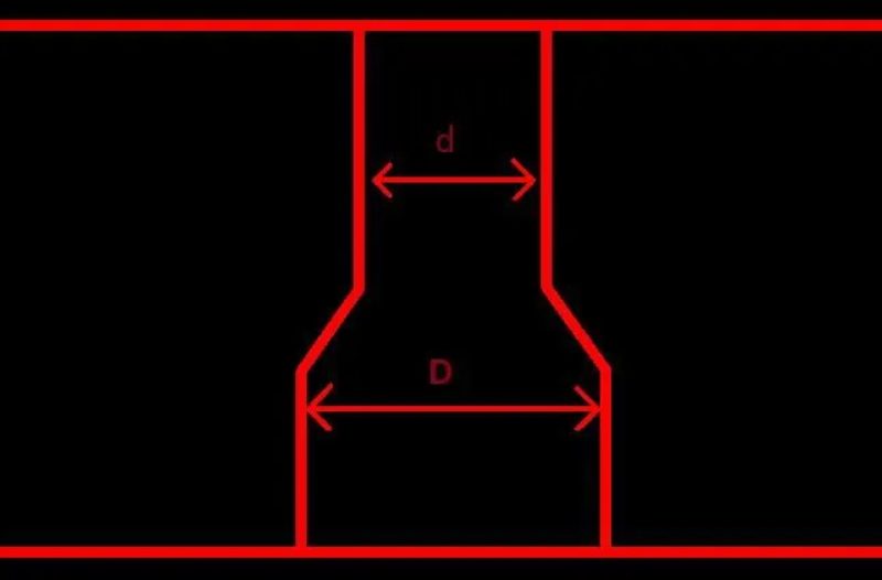
Backdrill size D > d Via hole size
This ensures that the hole removes the via stub but does not damage the surrounding copper or dielectric layers.
The backdrill process does not affect the layer stack up or no need to create special laminate as this is the post-fabrication process. After the final stack-up, plated-through holes are drilled and then the backdrill process is performed.
Below is a detailed step-by-step illustration of back drilling.
Step one: A through-hole via is drilled
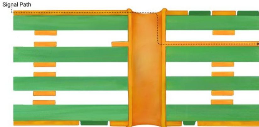
Step 1- Via barrel top to bottom
Step two: After the through-hole via is drilled, a back drill that has a diameter larger than the through-hole via will be drilled.
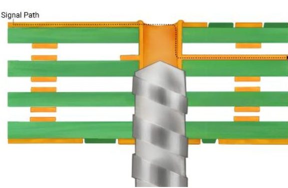
Step 2- Back drill hole breaking via barrel
Step three: After the backdrill, the unwanted wall of copper will be removed.
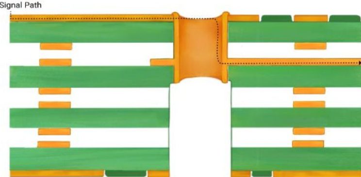
Step 3- After Back drill
The Factors Affect the Effectiveness of the Back Drilling in the Back Drill PCB
The factor that affects the effectiveness of the back drilling in the back drill PCB manufacturing. Before deciding to back drilling in your PCB design. There are several factors to consider:
- Board material and thickness
- Via size and spacing
- Trace and pad clearance
The effectiveness of the back-drilling process can be influenced by the material and the thickness of the PCB in the Back drill PCB manufacturing. For example, FR-4, Ceramic or Metal back PCB may require different drill bits and drilling parameters due to the hardness and thermal conductivity.
The size and spacing of the vias can also affect the effectiveness of the back drilling process. Smaller vias may require more precise drilling while larger vias may require larger drill bit or multiple passes. In some cases, Insufficient clearance causes the drill bit to accidentally drill through the plane or trace layer damaging the board. Trace and pad clearance from the back drill should be more than 10mil. The back drill does not overlap copper traces or be padded on any back drill layer.
In PCB backdrill manufacturing, special technical analysis or stack-up generation is required how to build the board in manufacturing. As this is an advanced technology not every manufacturer can do the PCB backdrill process as this process requires special machinery and multiple processes.
KKPCB provides global customers with one-stop services from PCB layout, prototype PCB proofing, PCB manufacturing, PCBA processing (including SMT and DIP), PCBA testing, PCBA product assembly and outbound packaging. You could provide a Gerber file or BOM list to us, we will offer the finished PCB products or PCB assembly which are satisfied with you.

