Understanding BGA PCB Assembly
Ball Grid Array (BGA) technology has revolutionized the world of circuit board assembly, providing a reliable and efficient method for mounting components on printed circuit boards (PCBs). In this blog, we will explore the basics of BGA PCB assembly, discussing why it is so popular in modern electronics, the detailed process of mounting BGAs, and key considerations to keep in mind.
What is BGA Assembly?
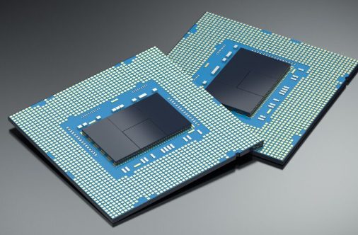
BGA assembly refers to the process of attaching a ball grid array (BGA) to a circuit board using a solder reflow process. BGAs are surface mount components that use an array of solder balls to create electrical interconnections between components and PCBs. The technology is used in a wide range of electronic devices, from smartphones and laptops to high-end servers and telecommunications equipment.
Why BGA?
The main reasons for the widespread adoption of BGA PCB assembly technology include:
High Density: BGAs enable higher density connections than traditional leaded components. This is especially important as devices become more compact and complex.
Improved Performance: Due to its design, BGAs have better electrical and thermal performance, which is critical for high-speed, high-power applications.
Reliability: Solder balls provide a more robust connection that can withstand mechanical stress and vibration better than traditional leads.
BGA Assembly Process
The process of mounting a BGA onto a PCB involves several critical steps to ensure that the final product is reliable and functional. Each step is described in detail below:

PCB Design and Preparation
Before you begin BGA assembly, you must design the PCB to accommodate the specific BGA component. This involves creating a layout that includes pads for each solder ball on the BGA. Proper spacing and pad design are critical to preventing issues such as bridging or insufficient solder joints.
Solder Paste Application
Once the BGA PCB component design is complete, solder paste is applied to the pads where the BGA will be placed. This is typically done using a stencil to ensure precise application. Solder paste consists of tiny solder particles suspended in a flux medium that aids in the reflow process.
Component Placement
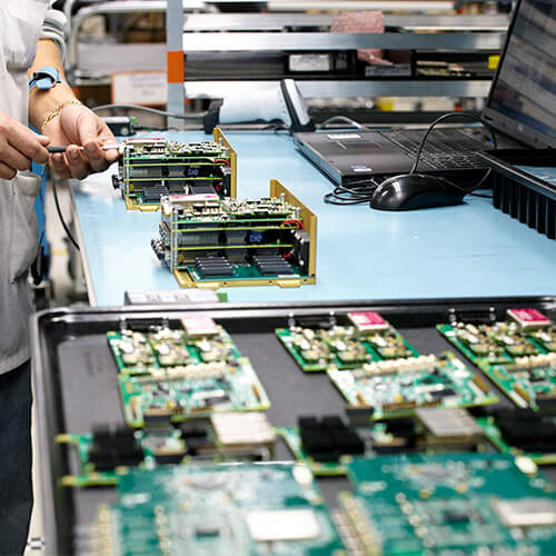
Once the solder paste is in place, the BGA PCB assembly components are carefully placed onto the PCB. This step typically uses an automated pick and place machine to ensure accuracy and efficiency. The solder balls on the BGA are aligned with the corresponding pads on the PCB.
Reflow Soldering
The assembled PCB is then fed into a reflow oven where it is gradually heated to melt the solder paste and form a strong solder joint between the BGA and the PCB. This step is critical because an improper reflow profile can lead to defects such as voids, incomplete reflow, or thermal damage to components.
Inspection and Quality Control
After reflow soldering, the assembled PCB undergoes rigorous inspection and quality control checks. Techniques such as X-ray inspection can be used to verify the integrity of the solder joints, especially since BGAs have hidden connections that are not visible to the naked eye. Automated Optical Inspection (AOI) systems can also be used to check for surface defects.
BGA Assembly Capabilities
| Capability | Standard |
|---|---|
| Types of BGA PCB: | Micro Ball Grid Array (MBGA)Thin Chip Array Ball Grid Array (CTBGA)Chip Array Ball Grid Array (CABGA)Very Thin Chip Array Ball Grid Array (CVBGA)Very Fine Pitch Ball Grid Array (VFBGA)Land Grid Array (LGA)Chip scale Package (CSP)Wafer level chip scale packaging (WLCSP) |
| Size: | Available in custom size. |
| PCB Testing Protocols: | X-ray inspectionFunctional TestingAutomated Optical Inspection |
| BGA rework: | PCB ReballingPad and Track RepairBGA Site ModificationCorrecting Damaged or Missing BGA padsComponent removal and replacementBGA Assembly |
Key Considerations for BGA Assembly
While BGA technology offers many advantages, successful implementation requires careful attention to several factors:
Design for Manufacturability (DFM)
DFM principles should be applied during the PCB design phase to ensure that the layout is optimized for BGA assembly. This includes proper pad design, adequate spacing, and consideration of thermal profile requirements for reflow soldering.
Solder Paste Quality
The quality of solder paste and its application play an important role in the success of BGA assembly. Consistent stencil thickness, proper solder paste composition, and controlled application are critical to avoid common problems such as solder bridging or insufficient solder.
Reflow Temperature Profile
A well-defined reflow profile is critical to ensure that the solder paste melts and solidifies properly without damaging the components. Factors such as peak temperature, heating rate, and cooling rate must be carefully controlled.
Inspection and Testing
Given the hidden nature of BGA connections, thorough inspection and testing must be performed to ensure reliable performance. X-ray inspection is the most effective method for detecting hidden defects, while functional testing can verify the overall performance of the assembled PCB.
BGA PCB assembly is a complex process that plays a vital role in modern electronics manufacturing. BGA technology, with its high-density connections, improved performance, and reliability, is essential for manufacturing compact and powerful electronic devices.
KKPCB conducts research on special processing technologies such as ordinary double-sided boards, thick copper circuit boards, high-frequency circuit boards, HDI circuit boards, rigid-flexible circuit boards, FPC flexible boards, buried blind hole circuit boards, and IC carrier boards. Provides PCB design, PCB layout, PCB prototyping and PCB assembly services.


