


Through-Hole Pad Design: Enhancing PCB Durability and Reliability
In printed circuit board (PCB) design, the choice of pad type plays a critical role in determining the durability, reliability, and performance of the final product. Through-hole pads, which are designed for components with leads that pass through the PCB, offer superior mechanical and electrical connections compared to surface mount pads. This article explores the design steps for through-hole pads, their advantages, and how they compare to surface mount technology.
Through-Hole Pad Design: Key Steps
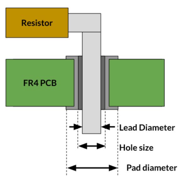
Through-hole pad design involves calculating the appropriate hole size and pad diameter to ensure a secure mechanical and electrical connection. The following table outlines the steps and formulas for designing through-hole pads:
| Step | Description | Formula | Notes |
|---|---|---|---|
| 1 | Determine maximum lead diameter | – | Check component datasheet. Consider wire shape (round, square, rectangular). |
| 2 | Calculate minimum hole size | Minimum hole size = maximum lead diameter + hole diameter factor | Factor: +0.25mm (A), +0.20mm (B), +0.15mm (C) |
| 3 | Calculate pad diameter | Pad diameter = minimum hole size + 0.1mm + minimum manufacturing allowance | Allowance: +0.40mm (A), +0.25mm (B), +0.20mm (C) |
Step-by-Step Guide to Through-Hole Pad Design
- Determine Maximum Lead Diameter:
- Refer to the component datasheet to find the maximum lead diameter.
- For square or rectangular leads, use the diagonal measurement as the hole diameter.
- Calculate Minimum Hole Size:
- Add a hole diameter factor to the maximum lead diameter based on the density class:
- Density Class A (General Design): +0.25 mm
- Density Class B (Medium Design): +0.20 mm
- Density Class C (High-Density Design): +0.15 mm
- Add a hole diameter factor to the maximum lead diameter based on the density class:
- Calculate Pad Diameter:
- Combine the minimum hole size with the minimum annular ring measurement and manufacturing allowance:
- Density Class A: +0.40 mm
- Density Class B: +0.25 mm
- Density Class C: +0.20 mm
- Combine the minimum hole size with the minimum annular ring measurement and manufacturing allowance:
What is an Annular Ring?
The annular ring is the conductive (usually copper) area surrounding the PCB hole. It ensures a strong connection between the PCB and the component leads inserted into the holes. A properly designed annular ring is critical for mechanical strength and electrical reliability.
Through-Hole Assembly Process
Through-hole assembly involves inserting the leaded component into the through-hole pad and soldering it on the opposite side of the board. This process can be done manually or using automated soldering machines. Through-hole pads can be either:
- Plated Through-Hole (PTH): The hole is plated with conductive material to create an electrical connection between layers.
- Non-Plated Through-Hole (NPTH): The hole is not plated, used primarily for mechanical mounting.
Through-Hole vs. Surface Mount Pads
Advantages of Through-Hole Pads:
- Durability: Through-hole components provide stronger mechanical bonds, making them ideal for heavy or high-stress components such as electrolytic capacitors, relays, and connectors.
- Ease of Prototyping: Through-hole components are easier to adjust, replace, and probe with debugging tools like oscilloscopes.
- Thermal Management: Through-hole pads are better suited for components that dissipate significant heat, as the leads can transfer heat to the PCB more effectively.
Advantages of Surface Mount Pads:
- Compact Design: Surface mount technology (SMT) allows for smaller components and higher part density, enabling more functionality in a smaller space.
- Multi-Layer Boards: SMT is ideal for complex, multi-layer PCB designs.
- Cost-Effective for Mass Production: SMT is faster and more cost-effective for high-volume production.
Limitations:
- Through-Hole: Larger holes and leads can limit routing space on multi-layer boards.
- Surface Mount: Less suitable for high-heat components and may require specialized equipment for assembly and rework.
Applications of Through-Hole Pads
Through-hole technology is commonly used for:
- Heavy components like transformers and large capacitors.
- High-reliability applications such as aerospace and automotive electronics.
- Prototyping and debugging, where components may need to be replaced or adjusted frequently.
Through-hole pad design is a critical aspect of PCB development, offering enhanced durability and reliability for components that require strong mechanical and electrical connections. By following the design steps outlined above, engineers can ensure proper pad sizing and annular ring dimensions, leading to robust and long-lasting PCB assemblies. While surface mount technology offers advantages in compactness and production efficiency, through-hole pads remain indispensable for applications requiring strength, thermal management, and ease of prototyping.
KKPCB provides end-to-end PCB solutions, from design support and rapid prototyping to mass production of HDI, rigid-flex, aluminum, and RF circuit boards. Serving global clients across telecommunications, automotive, industrial, medical, aerospace, and instrumentation sectors, we specialize in solving complex PCB challenges with advanced technologies such as HDI structures (1+N+1, 2+N+2, 3+N+3), embedded/blind vias, and multilayer designs. Utilizing high-TG materials and low Dk/Df dielectrics, we ensure superior performance and reliability. Our manufacturing adheres to IPC-6012 Class 3 standards and holds ISO 9001, IATF 16949, UL, and other international certifications, guaranteeing compliance with industry requirements.