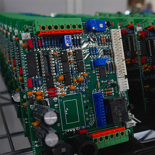
The Significance of Impedance in PCB Design and Manufacturing
Impedance plays a critical role in the functionality, reliability, and performance of printed circuit boards (PCBs). Understanding and managing impedance is essential for ensuring proper signal transmission and maintaining the integrity of the electronic devices that rely on these boards. Below is a detailed analysis of impedance and its importance in PCB design and manufacturing.
1. What is Impedance?
Impedance is a combination of resistance and reactance, which determines how a circuit resists the flow of alternating current (AC). In PCBs, impedance affects:
- Signal transmission quality: Ensuring minimal distortion and loss.
- Conductivity: Directly tied to the efficiency of the electrical path.
To maintain optimal performance, the impedance of PCBs must be as low as possible, with resistivity ideally lower than 1×10⁻⁶ Ω·cm².
2. Why Do PCBs Need Low Impedance?
a. Signal Integrity
Low impedance minimizes signal distortion and maintains consistent signal levels, crucial for high-frequency and high-speed circuits.
- High Impedance Issues: Causes signal reflections, losses, and delays, which degrade the performance of digital circuits.
- Characteristic Impedance: Maintaining consistent impedance along signal traces ensures signal integrity, especially in RF or high-speed designs.
b. Electrical Conductivity
Low impedance ensures better current flow, reducing power loss and heating. This is particularly important for power distribution layers and high-current applications.
c. Manufacturing Quality
During PCB production, various processes (e.g., copper deposition, tin plating) must maintain low resistivity to ensure the board’s overall impedance meets design specifications. If not, the circuit board may fail or degrade over time.
3. The Impact of Tinning on Impedance
a. The Role of Tin Plating
Tin plating is applied to solder joints to facilitate connections between copper traces and electronic components. However, the quality and purity of the tin layer directly influence impedance.
b. Common Issues in Tin Plating
- Impurities: Tin compounds (e.g., oxides or halides) increase impedance, reducing conductivity.
- Discoloration and Oxidation: Chemical reactions cause surface degradation, increasing resistance over time.
- Tin Whiskers: These microscopic metal filaments can lead to short circuits and failures.
- Poor Solderability: Low-quality tin layers complicate soldering, leading to weak joints.
c. Advances in Chemical Tinning
Chemical tinning has gained popularity for its uniform application. Industry leaders like Kunming University of Science and Technology and Guangzhou Tongqian Chemical have developed methods to produce pure, low-resistivity tin layers. High-quality chemical tinning ensures:
- Low resistivity for better conductivity.
- Stable performance over time, resisting discoloration and oxidation.
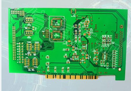
4. Impedance Challenges in PCB Manufacturing
a. Variability Over Time
Impedance can change due to environmental factors like humidity, leading to oxidation and electrolysis of the tin layer. These changes:
- Increase resistivity.
- Degrade signal transmission.
- Impact the overall performance of the PCB.
b. Hidden Issues
- Invisibility: Impurities and oxidation are not visible to the naked eye.
- Measurement Challenges: Impedance changes dynamically with time and environmental conditions, making continuous monitoring difficult.
c. Distributed Capacitance
Impedance mismatches may introduce unintended capacitance in the circuit, further affecting signal quality.
5. Practical Implications for the Electronics Industry
a. Quality Assurance
Manufacturers must rigorously test tin layers and their impedance properties to prevent future failures. The use of advanced testing methods and endurance trials helps detect potential issues.
b. Material Selection
Choosing high-purity tin and proper plating techniques reduces the risk of:
- High impedance.
- Tin whisker formation.
- Long-term degradation.
c. Impact of Low-Quality Tinning
Using subpar tin compounds leads to:
- Inconsistent impedance.
- Poor device reliability.
- Increased production costs due to higher failure rates.
6. Strategies to Optimize PCB Impedance
- Use Pure Tin Layers: Prioritize high-quality plating techniques to ensure low resistivity and consistent impedance.
- Implement Regular Testing: Conduct impedance testing at various stages of production and in post-production quality checks.
- Optimize Environmental Controls: Minimize exposure to humidity and contaminants during manufacturing and storage.
- Simulation Tools: Use software to simulate impedance behavior under various conditions, helping design more reliable PCBs.
7. Conclusion
The significance of impedance in PCBs cannot be overstated. From ensuring signal integrity to maintaining conductivity, low impedance is a cornerstone of reliable PCB design. By focusing on high-quality materials, advanced manufacturing techniques, and rigorous testing, manufacturers can minimize impedance-related issues and deliver high-performance PCBs for modern electronics.


