The Five Golden Rules of PCB Design
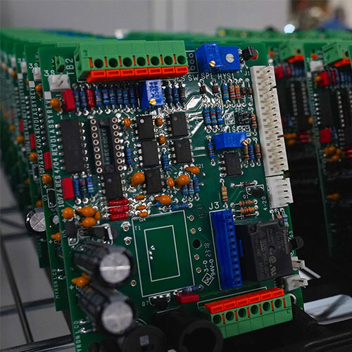
Printed Circuit Boards (PCBs) are the backbone of electronic circuits, organizing and supporting all circuit components. Effective PCB design not only assembles components efficiently but also prevents errors caused by manual wiring. This article highlights five essential PCB design principles that enhance power supply design and improve overall performance.

1. Maintain a Logical Direction
- Segregate Signals: Group inputs/outputs, AC/DC signals, high/low frequencies, and high/low voltages separately to prevent interference. Ideally, signal flow should be linear, avoiding loops where possible. Isolation measures can help improve performance in cases where linearity isn’t achievable.
2. Choose an Optimal Grounding Point
- Effective Grounding: Establishing a common grounding point is crucial for stability. For instance, connect multiple ground lines from the amplifier to the main ground to prevent interference. Though complete grounding uniformity can be challenging, following this rule as much as possible will benefit PCB performance.
3. Place Power Supply Filter and Decoupling Capacitors Correctly
- Proximity to Components: Ensure capacitors are placed close to the components they filter. Capacitors too far from the target components will lose effectiveness. Proper capacitor placement also reduces grounding issues.
4. Optimize Trace and Via Dimensions
- Line Width and Via Size: Thicker traces are preferable, especially for high-voltage and high-frequency signals. Smooth, rounded traces without sharp angles are ideal to minimize interference. Use large copper areas for grounding to prevent uneven corrosion and enhance circuit durability.
5. Minimize Vias, Manage Solder Joints, and Control Line Density
- Reduce Vias: Excessive vias can introduce quality issues during copper deposition, so use them sparingly. Keep parallel line spacing adequate to avoid unintentional connections during soldering. Ensure enough space between solder joints for easy, high-quality manual soldering.
Mastering these PCB design rules—like efficient grounding, proper trace sizing, and capacitor placement—significantly improves design quality and efficiency. By following these guidelines, you can reduce rework, save costs, and achieve more reliable, higher-quality PCB designs.
As a leading PCB manufacturer, members of our printed circuit board (PCB) design service team are practical partners working with you on every project and can help you achieve your goals at any time. They can complement your engineering expertise, which helps speed up time to market, reduce the time from concept to production, and ensure that quality is integrated into the manufacturing process to maximize your profits.


