Talk about high-frequency microwave printed circuit boards and aluminum substrates
In the past two or three years, the most fashionable technologies and products in our industry are HDI (high density interconnection) and Build-up Multilayer (build-up printed circuit board). However, in the development trend of market economy and high-tech products, there is another branch, which is high-frequency microwave printed circuit boards and metal-based printed circuit boards. Today, I will talk about these two issues.
1. High frequency microwave printed circuit board
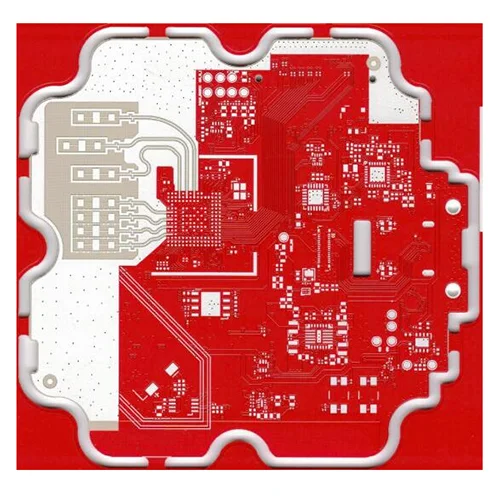
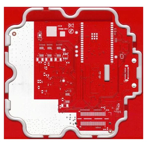
1. High-frequency microwave printed circuit boards are becoming popular in China.
In recent years, many PCB enterprises in East China, North China and the Pearl River Delta have been eyeing the high-frequency microwave board market, collecting dynamics and information on high-frequency waves and polytetrafluoroethylene (Teflon, PTFE), and considering this new type of PCB as an indispensable supporting product for the electronic information high-tech industry, and strengthening research and development. Some company bosses have identified high-frequency microwave boards as a new economic growth point for future companies.
Foreign experts predict that the market for high-frequency microwave boards will develop very quickly. In the fields of communications, medical treatment, military, automobiles, computers, instruments, etc., the demand for high-frequency microwave boards is rising rapidly. In a few years, high-frequency microwave boards may account for about 15% of the total global printed circuit boards. Many PCB companies in Taiwan, South Korea, Europe, the United States, and Japan have formulated development plans in this direction.
In the past two years, European and American high-frequency microwave board suppliers Rogers, Arlon, Taconic, Metclad, GIL and Chukoh have begun to enter the potential large market of China, looking for agents and teaching related technologies. The American GIL company held a lecture on “Application and Manufacturing Technology of High-Frequency Microwave Printed Boards” in Shenzhen. Hundreds of seats were full, and the corridors were also full of corporate representatives listening to the speeches. Many CEOs listened to the technical lectures for a whole day. I really didn’t expect that domestic peers would have such a strong interest in high-frequency boards. European and American board suppliers can provide more than 100 varieties of board series with dielectric constants ranging from 2.10, 2.15, 2.17, … to 4.5, or even higher.
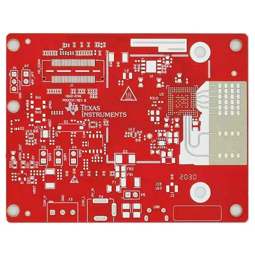
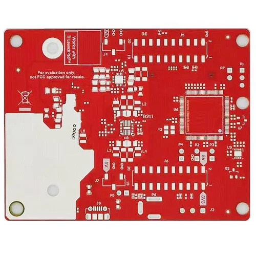
In the Pearl River Delta and the Yangtze River Delta, it is understood that many companies have advertised that they can place orders for Teflon and high-frequency boards in bulk. It is said that some companies have reached a monthly production level of several thousand square meters. The demand for high-frequency microwave boards from many domestic radar and communication research institutes is increasing year by year. The demand for high-frequency microwave printed boards from large domestic communication companies such as Huawei, Bell, and Wuhan Post and Telecommunications Research Institute is increasing year by year. Foreign companies engaged in high-frequency microwave products have also moved to China to purchase high-frequency microwave printed boards nearby. All signs indicate that high-frequency microwave boards have become popular in China.
(What is high frequency? Above 300MHZ, that is, the short-wave frequency range with a wavelength of more than 1 meter, is generally called high frequency.)
2.Why is it getting hot?
There are three reasons.
(1) Some frequency bands of high-frequency communications originally used for military purposes have been given to civilian use (starting in 1996), which has greatly developed civilian high-frequency communications. It has been widely used in various fields such as long-distance high-frequency communications, navigation, medical treatment, transportation, traffic, and warehousing.
(2) High confidentiality and high transmission quality have led to the development of mobile phones, car phones, and wireless communications towards high frequencies. High picture quality has enabled radio and television transmission to use very high frequencies and ultra-high frequencies to broadcast programs. The transmission of high amounts of information requires satellite communications, microwave communications, and optical fiber communications to be high frequencies.
(3) The increase in computer technology processing power and information memory capacity has urgently required high-speed signal transmission.
In short, the high frequency and high speed of electronic information products have put forward high requirements on the high-frequency characteristics of printed circuit boards.
3. Why is low ε (Dk) required for printed circuit boards?
ε or Dk, called dielectric constant, is the ratio of the capacitance when a certain substance is charged between electrodes to the capacitance of a vacuum capacitor of the same structure. It usually indicates the ability of a certain material to store electrical energy. When ε is large, the ability to store electrical energy is large, and the speed of electrical signal transmission in the circuit will be low. The direction of the current of the electrical signal passing through the printed circuit board is usually alternating between positive and negative, which is equivalent to the process of continuously charging and discharging the substrate. In the exchange, the capacitance will affect the transmission speed. And this effect is more important in high-speed transmission devices. Low ε means small storage capacity, fast charging and discharging process, and thus fast transmission speed. Therefore, in high-frequency transmission, a low dielectric constant is required.
There is another concept, which is dielectric loss. The energy consumed by dielectric materials due to heat under the action of alternating electric fields is called dielectric loss, which is usually expressed by the dielectric loss factor tanδ. ε and tanδ are proportional, and high-frequency circuits also require low ε and small dielectric loss tanδ, so that energy loss is also small.
4. ε of Teflon printed circuit board
Among printed circuit board substrates, the dielectric constant ε of polytetrafluoroethylene substrate is the lowest, typically only 2.6~2.7, while the dielectric constant ε of FR4, a general glass cloth epoxy resin substrate, is 4.6~5.0. Therefore, the signal transmission speed of Teflon printed circuit boards is much faster than that of FR4 (about 40%). The loss factor of Teflon board is 0.002, which is 10 times lower than FR4’s 0.02, and the energy loss is much smaller. In addition, polytetrafluoroethylene is called the “king of plastics” and has excellent electrical insulation properties, chemical stability and thermal stability (there is still no solvent that can dissolve it below 300°C). Therefore, high-frequency and high-speed signal transmission must first use Teflon or other substrates with low dielectric constants. I have seen that Polyflon, Rogers, Taconic, Arlon, and Meclad can all provide substrates with dielectric constants of 2.10, 2.15, 2.17, and 2.20, and their dielectric loss factors are 0.0005~0.0009 at 10GHZ. PTFE substrates have very good performance, but the process of processing them into printed circuit boards is completely different from that of traditional FR4, which will be discussed later.
In the past two years, in practice, in addition to those requiring ε of 2.15 and 2.6, we also often use Rogers RO4000, GIL1000 series, etc. with ε3.38, 3.0, 3.2, 3.8, etc.
5. Basic requirements for high-frequency microwave boards
·Due to high-frequency signal transmission, the characteristic impedance of the finished printed circuit board conductor is strictly required, and the line width of the board is usually required to be ±0.02mm (the most stringent is ±0.015mm). Therefore, the etching process needs to be strictly controlled, and the film used for optical imaging transfer needs to be compensated according to the line width and copper foil thickness.
The lines of this type of printed circuit board do not transmit current, but high-frequency electric pulse signals. Defects such as pits, gaps, pinholes, etc. on the wires will affect the transmission. Any such small defects are not allowed. Sometimes, the thickness of the solder mask is also strictly controlled. If the solder mask on the line is too thick or too thin by a few microns, it will be judged as unqualified.
·Thermal shock 288℃, 10 seconds, 1~3 times, no hole wall separation occurs. For polytetrafluoroethylene boards, it is necessary to solve the wettability in the hole, make sure there are no holes in the chemical copper deposition hole, and the copper layer electroplated in the hole can withstand thermal shock. This is one of the difficulties in making Teflon hole-plated boards. Because of this, many substrate manufacturers have developed and produced alternatives with a higher ε, and the same chemical copper deposition process as conventional FR4. Rogers Ro4003 (ε3.38) and Xi’an 704 Factory’s LGC-046 (ε3.2±0.1) are such products.
Warpage: Usually the finished board is required to be 0.5~0.7%.
6. Difficulties in processing high-frequency microwave boards
Due to the physical and chemical properties of polytetrafluoroethylene sheets, their processing technology is different from the traditional FR4 process. If it is processed under the same conditions as conventional epoxy resin glass fiber copper clad laminates, qualified products cannot be obtained.
(1) Drilling: The substrate is soft, so the number of stacked boards should be small. Usually, two boards with a thickness of 0.8 mm should be stacked. The rotation speed should be slow. A new drill bit should be used. The drill bit top angle and thread angle have special requirements.
(2) Printing solder mask: After the board is etched, the board should not be polished with a roller brush before printing solder mask green oil to avoid damaging the substrate. Chemical methods are recommended for surface treatment. To achieve this: without polishing the board, the circuit and copper surface are uniform and there is no oxide layer after printing solder mask, which is not easy.
(3) Hot air leveling: Based on the inherent properties of fluororesin, rapid heating of the board should be avoided as much as possible. Before tin spraying, it should be preheated at 150°C for about 30 minutes, and then tin spraying should be performed immediately. The temperature of the tin tank should not exceed 245°C, otherwise the adhesion of the isolated pad will be affected.
(4) Milling shape: Fluorine resin is soft, and ordinary milling cutters have a lot of burrs and are uneven when milling the shape. It is necessary to use a suitable special milling cutter to mill the shape.
(5) Transportation between processes: Do not place it vertically, only place it flat in a basket with paper between them. Do not touch the circuit graphics on the board with your fingers during the whole process. Prevent scratches and scratches during the whole process. Scratches, pinholes, indentations, and pits on the circuit will affect signal transmission and the board will be rejected.
(6) Etching: Strictly control side etching, serrations, and notches. The line width tolerance is strictly controlled to ±0.02mm. Check with a 100x magnifying glass.
(7) Chemical copper plating: The pretreatment of chemical copper plating is the biggest difficulty in manufacturing Teflon boards and it is also the most critical step. There are many methods for copper plating pretreatment, but in summary, there are only two methods that can stabilize the quality and are suitable for mass production:
Method 1: Chemical method: Sodium metal is added to tetrahydrofuran and other solutions to form a sodium-tetrafluoroethylene complex, so that the surface atoms of polytetrafluoroethylene in the hole are etched to achieve the purpose of wetting the hole. This is a classic and successful method with good results and stable quality, but it is highly toxic, and sodium metal is flammable and dangerous, so it needs to be managed by a dedicated person.
Method 2: Plasma method: Special imported equipment is required. In a vacuum environment, carbon tetrafluoride (CF4) or argon (Ar2) nitrogen (N2), oxygen (O2) gas is injected between two high-voltage electrodes. The printed circuit board is placed between the two electrodes, and plasma is formed in the cavity, thereby removing the drilling dirt and dirt in the hole. This method can obtain satisfactory and uniform results, and mass production is feasible. However, it requires investment in expensive equipment (about more than 100,000 US dollars per machine). There are two famous plasma equipment companies in the United States: APS and March.
In recent years, some domestic literature has also introduced many other methods, but the classic and effective methods are the two mentioned above.
For ε3.38 and Rogers Ro4003 high-frequency substrates, they have similar high-frequency performance to polytetrafluoroethylene glass fiber substrates, and are easy to process like FR4 substrates. This is a high-heat-resistant material with glass fiber and ceramic as fillers and a glass transition temperature of Tg>280℃. Drilling holes in this substrate consumes a lot of drill bits, and special drilling machine parameters are required. The milling cutter must be changed frequently for milling shapes; but other processing techniques are similar and no special hole processing is required, so it has been recognized by many PCB factories and customers. However, Ro4003 does not contain flame retardants, and the board can cause combustion when it reaches 371℃. The state-owned 704 factory LGC-046 board is a modified polyphenylene ether (PPO) type with a dielectric constant of 3.2 and the same processing performance as FR4. This product has also been recognized and used by many singles in China.
7.Where are high frequency microwave boards used?
Satellite receivers, base antennas, microwave transmission, car phones, global positioning systems, satellite communications, communication equipment adapters , receivers, signal oscillators, home appliance networking, high-speed computers, oscilloscopes, IC test instruments, etc., high-frequency communications, high-speed transmission, high confidentiality, high transmission quality, high memory capacity processing and other communication and computer fields all require high-frequency microwave printed circuit boards.
8. Overview of high-frequency microwave panels at home and abroad
Domestically, in addition to the above-mentioned 704 factory LGC-046 modified polyphenylene ether sheet, Taizhou high-frequency copper foil sheet factory TF-2, F4B, F4BK high-frequency microwave, polytetrafluoroethylene sheet is also selling very well. It is said that many companies in Beijing, the Yangtze River Delta, and Guangdong are also starting up and starting production.
Abroad, the main board suppliers are: Rogers, Arlon, GIL Taconic, Metclad, Isola, Polyclad in Europe and the United States, Asaki, Hitach, Ehemical, Chukok in Japan, etc., which have formed about 130 varieties of paper with different dielectric constants for high-frequency microwaves.
The current gap between China and foreign countries: variety, quality consistency, price; it is difficult for major foreign customers to recognize Chinese products, etc.
The thickness of the sheet is not often used, 1.5~1.6mm, while 0.5, 0.8, 1.0mm are more common, mainly considering the cost. The price of Teflon sheet is 5~10 times that of ordinary FR4, and bulk purchases also cost about $100/m2, and small purchases cost several hundred dollars/m2.
Summary: High-frequency microwave plates should be a new product of high-tech. With the continuous development of communications and computers towards high frequency and high speed, their uses will become wider and wider in the future. The plate price is also high, with a large profit margin. This product has a bright future.
2. Aluminum substrate
1. Why use metal-based printed circuit boards?
(1) Heat dissipation
At present, many double-sided boards and multi-layer boards have high density and high power, and it is difficult to dissipate heat. Conventional printed circuit board substrates such as FR4 and CEM3 are poor conductors of heat, with insulation between layers, and heat cannot be dissipated. If local heating of electronic equipment is not eliminated, it will cause high-temperature failure of electronic components. Metal-based printed circuit boards can solve this heat dissipation problem.
(2) Thermal expansion
Thermal expansion and contraction are the common nature of matter. Different substances have different CTE (Coefficient of thermal expansion).
Printed circuit boards are a composite of resin + reinforcing material (such as glass fiber) + copper foil. In the XY axis direction of the board surface, the thermal expansion coefficient (CTE) of the printed circuit board is 13~18 PPM/℃, and in the Z axis direction of the board thickness, it is 80~90PPM/℃, while the CTE of copper is 16.8PPM/℃. The CTE of the sheet ceramic chip carrier is 6PPM/℃. The CTE of the metallized hole wall and the connected insulating wall of the printed circuit board in the Z axis is very different. The heat generated cannot be removed in time, and the thermal expansion and contraction cause the metallized hole to crack and disconnect, so the machine equipment is unreliable.
SMT (surface mount technology) makes this problem more prominent and becomes a problem that must be solved. Because the surface mount interconnection is achieved through direct connection of surface solder joints, the CTE of the ceramic chip carrier is 6, while the CTE of the FR4 substrate in the XY direction is 13~18. Therefore, due to the different CTE, the mounting connection solder joints will be subjected to stress for a long time and will cause fatigue fracture.
Metal-based printed circuit boards can effectively solve the heat dissipation problem, thereby alleviating the thermal expansion and contraction problem of different materials of components on the printed circuit board, and improving the durability and reliability of the whole machine and electronic equipment.
(3) Dimensional stability
Metal-based printed circuit boards are obviously much more stable in size than printed circuit boards made of insulating materials. Aluminum-based printed circuit boards and aluminum sandwich panels change in size by 2.5-3.0% when heated from 30°C to 140-150°C.
(4) Other reasons
Iron-based printed circuit boards have a shielding effect; they replace brittle ceramic substrates; they can safely use surface mounting technology; they reduce the effective area of the printed circuit board; they replace components such as heat sinks, improve the product’s heat resistance and physical properties; and they reduce production costs and labor.
2. Brief History
Metal-based printed circuit boards, as a category of printed circuit boards, were first used in the early 1960s, and were pioneered in the United States. In 1963, Veslem Electrico Company in the United States made iron-based sandwich printed circuit boards and applied them to relays. In 1964, the number of metal-based printed circuit boards in the United States reached 1 million. The book “Copper-clad Laminates for Printed Circuits” (October 2001) compiled and published by the National Copper-clad Laminate Industry Association said that in 1969, Japan’s Sanyo Company first invented the manufacturing technology of aluminum-based copper-clad laminates, and in 1974, it began to be used in STK series power amplifier hybrid integrated circuits. This is different from the literature I found. In any case, it was the United States and Japan that first used metal-based printed circuits in the 1960s.
In the 1960s and 1970s, the Ministry of International Trade and Industry of Japan conducted a lot of investigations and recognized that the difficulty faced by the use of PCBs is that when high-density assembly is performed, the assembly density of components is high, and heat dissipation is a big problem. Ordinary paper, glass cloth, and epoxy copper clad laminates are insulating materials with low thermal conductivity and are not suitable for heat dissipation. When the multi-layer board has many layers, high density, and high power, the heat will definitely not be removed. Therefore, metal-based printed circuit boards must be used. Japanese companies such as Sumitomo and Matsushita Electric have launched many commercialized metal-based copper clad laminates.
In the 1980s and 1990s, metal substrates were widely adopted in countries around the world. It is estimated that the annual output value of metal-based printing in the world is about 2 billion US dollars. Japan’s output value was 2.5 billion in 1991, 6 billion in 1996, and 8 billion yen in 2001. Bergquist in the United States is a company specializing in aluminum-based copper-clad laminates. It claims to sell 30 million US dollars of such panels each year and has more than half of the market share in the United States. Companies such as Texas and Cleveland TechTrade in the United States have done a lot of research on metal substrates and have also produced products. In 1986, China began to develop iron-based copper-clad laminates for military use by the state-owned 704 Factory. However, I have reviewed the papers presented at the National Printed Circuit Academic Conferences and found that the earliest article was published by Chengdu 1010 Institute at the Second National Printed Circuit Academic Annual Conference in November 1983. The title was “Summary of Metal-Based Printed Circuit Board Manufacturing Process Tests”, and the products were also used in military products. Four years later, at the 3rd National Annual Academic Conference on Printed Circuits in Chengdu in September 1987, the 10th Institute of the Ministry of Electronics published another paper entitled “Design, Manufacturing and Application of Aluminum-Based Printed Circuit Boards”, indicating that the 10th Institute and Factory 704 had done a lot of work on aluminum substrates in the early years.
With the rapid development of China’s information electronics industry, metal-based printed circuit boards will be increasingly used in electronics, telecommunications, automobiles, motorcycles, power supplies, audio and other products in recent years. Due to the development of the market and technology, the heat dissipation problem has reached a point where it must be solved, and metal-based printing can show its strength.
3. Structure
The standard metal-based copper-clad laminates currently available on the market are composed of three layers of different materials: copper, insulation layer, and metal plate (copper, aluminum, and steel plate), and aluminum-based copper-clad laminates are the most common.
(1) Metal substrate
Aluminum-based substrate, using LF, L4M, Ly12 aluminum materials, requires expansion strength of 30kgf/mm2 and elongation of 5%. American Bergs aluminum-based substrate is divided into 4 types: 1.0, 1.6, 2.0, 3.2mm, and the aluminum model is 6061T6 or 5052H34. Japanese Panasonic Electric, Sumitomo R-0710, R-0771, AL C-1401, AL C-1370 and other models are aluminum-based copper-clad laminates, and the aluminum base thickness is 1.0~3.2mm.
Copper-based substrate, expansion strength of 25~32kgf/mm2, elongation of 15%. American Bergs copper-based substrate is divided into 5 thicknesses: 1.0, 1.6, 2.0, 2.36, 3.2mm, which is C11000 copper alloy.
Iron-based substrate, using cold-rolled copper plate, low-carbon copper, has magnetic shielding properties, thickness 0.5~1.5mm. Bergs uses invar (nickel-iron alloy), tungsten-gold alloy, and cold-rolled copper with thicknesses of 1.0 and 2.3 mm.
(2) Insulation layer
It acts as an insulation layer, usually 50~200um. If it is too thick, it can act as an insulator and prevent short circuits with the metal base, but it will affect the heat dissipation; if it is too thin, it can dissipate heat well, but it is easy to cause short circuits between the metal core and the component leads.
The insulation layer (or prepreg) is placed on an anodized and insulated aluminum plate, and is firmly bonded together with the copper layer on the surface through lamination.
Bergs has applied for a patent for its insulation layer. The standard aluminum substrate has an insulation layer of 75 microns, while the special type has an insulation layer of 150 microns.
(3) Copper
foil The back of the copper foil is chemically oxidized, and the surface is galvanized and brass-plated to increase the peel strength. The copper thickness is usually 0.5 and 1.2 tsp. Bergs uses ED copper, which has five types of copper thicknesses: 1, 2, 3, 4, and 6 tsp. The aluminum substrates we make for communication power supplies use 4-cup copper foil (140 microns).
The standard sizes of aluminum substrates provided by the United States are two: 16″×19″ and 18″×24″. Usable area: minus one inch. The aluminum substrates can also be divided into those with or without protective film.
4. Manufacturing Difficulties
The manufacturing of aluminum substrates with a copper thickness of 4.5OZ will encounter the following difficulties:
(1) Engineering design line width compensation: Because of the copper thickness, the line width must be compensated to a certain extent, otherwise the line width after etching will be out of tolerance and customers will not accept it. The line width compensation value needs experience accumulation.
(2) Uniformity of solder mask printing: Because the copper thickness of the circuit after graphic etching is out of the norm, it is very difficult to print solder mask. Customers will not accept skipped printing, too thick or too thin. How to print this layer of green oil well is also one of the difficulties.
(3) Etching: The line width after etching must meet the requirements of the customer’s drawings. Residual copper is not allowed, and it cannot be scraped off with a knife. Moving a knife will scratch the insulation layer, causing sparks and leakage during the withstand voltage test.
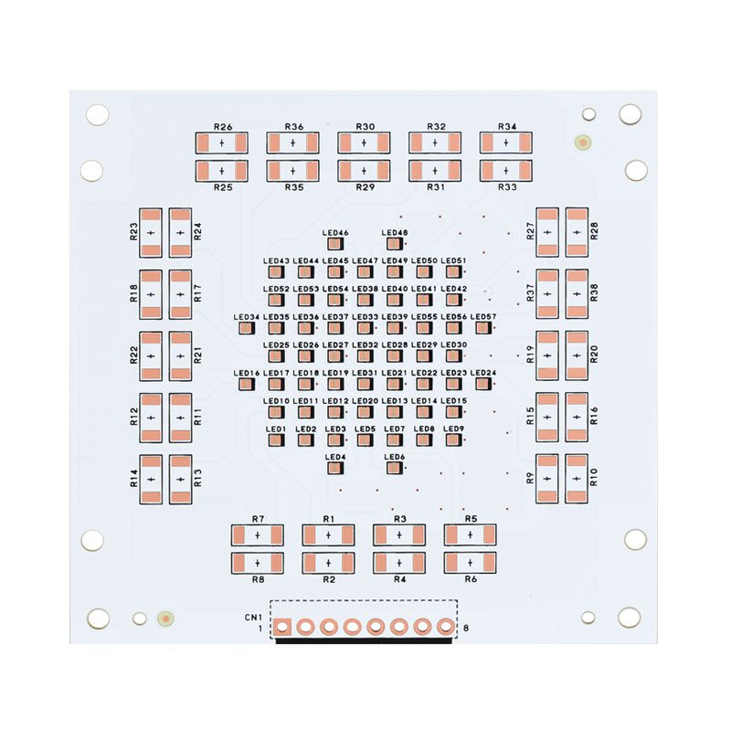
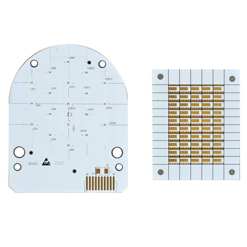
(4) Machining: Aluminum substrates can be drilled, but no burrs are allowed on the edge of the hole after drilling, which will affect the withstand voltage test. Milling the shape is very difficult. And punching the shape requires the use of advanced molds, and mold making requires skills, which is also one of the difficulties in making aluminum substrates. After the shape is punched, the edge is required to be very neat, without any burrs, and the solder mask layer on the edge of the board should not be damaged. Usually, a military mold is used, the holes are punched from the circuit, the shape is punched from the aluminum surface, and the force applied when the circuit board is punched is shearing from the top and pulling from the bottom, etc. These are all skills. After punching the shape, the warpage of the board should be less than 0.5%.
(5) The aluminum base surface must not be scratched during the entire production process: the aluminum base surface will change color or turn black when touched by hand or exposed to certain chemicals, which is absolutely unacceptable. Some customers will not accept the aluminum base surface being re-polished, so not scratching or touching the aluminum base surface during the entire process is one of the difficulties in producing aluminum substrates. Some companies use passivation technology, and some apply protective film before and after hot air leveling (spray tin)… There are many small tricks, and each one shows its magical powers.
(6) Over-high voltage test: Communication power aluminum substrates require 100% high voltage testing. Some customers require direct current, while others require alternating current. The voltage requirements are 1500V and 1600V, and the time is 5 seconds and 10 seconds, and 100% of the printed circuit boards are tested. Dirt on the board surface, burrs on the edges of holes and aluminum substrates, line serrations, and any damage to the insulation layer will cause fire, leakage, and breakdown during the high voltage test. The boards that are delaminated or bubbled during the voltage test are rejected.
The above are all production and process difficulties that must be overcome in the production of single-sided aluminum substrates. At present, some units make aluminum core printed circuit boards, that is, double-sided aluminum printed circuit boards, and blind hole multi-layer aluminum substrates, which are used in the automotive, communication, and instrumentation industries. I will not describe them one by one here.
5. Main performance:
The “Chinese Index” in the table above is recorded from the book “Copper Clad Laminates for Printed Circuits” (2001.10) P373. In addition, in order to apply for UL certification of aluminum substrates, it costs about 25,000 to 30,000 RMB, which is much more expensive than the usual UL certification of printed circuit boards. In addition, we have destroyed many aluminum substrates that have been broken down. To find out the reasons for the breakdown, we found that the insulating dielectric layer is only resin, fiber-free, 75 microns thick, and evenly coated; any pinholes, particles, black spots, and garbage on the insulating layer are the cause of the aluminum substrate being broken down by high voltage, so the environmental control of the insulating layer coating is very important.
It is obvious from the table above that all indicators of American products are higher than those of domestic products. This is probably one of the reasons why major domestic communication customers still do not recognize domestic aluminum-based panels.
Substrate appearance: Any obvious scratches, nicks, pinholes, pits, or streaky abrasion marks on the aluminum substrate are not acceptable.
6. Applications and Suppliers:
Application areas:
Communication power supply: voltage stabilizer, regulator, DC-AC adapter;
electronic control: relay, transistor base, cooling of components in various circuits;
switches, microwaves: radiator, insulation heat conduction of semiconductor devices, motor controller;
industrial automobiles: igniter, voltage regulator, automatic safety control system, lighting conversion system;
computers: power supply unit, floppy disk drive, motherboard;
home appliances: input-output amplifier, audio, power balance amplifier, etc.
Availability
The metal-based market is expanding year by year in China, and many foreign electronic assemblers are also investing in building factories in China, so the business opportunities are unlimited. At present, there are many factories in the Pearl River Delta that make aluminum substrates, and aluminum substrates used in communication power supplies are still using imported substrates. Although the price of domestically produced ones is cheap, it is said that none of them can be recognized after many attempts. Several factories in the Pearl River Delta currently have a monthly output of tens or hundreds of K, and the estimated output is hundreds of square meters. Gradually accumulated a lot of experience in mass production.

