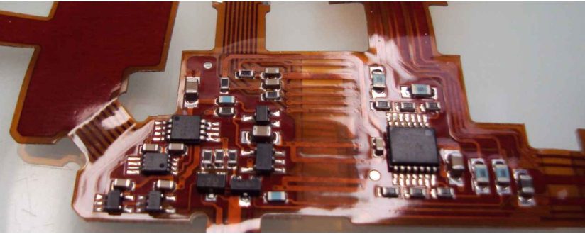
Flexible printed circuit boards (flexible PCBs or flex circuits) are made from flexible insulating materials such as polyimide film. Unlike traditional rigid PCBs, flexible PCBs can bend and twist while maintaining electrical connectivity, making them ideal for space-constrained and dynamic applications.
Key Takeaways
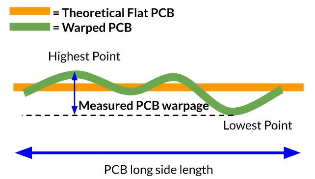
Stress during fabrication, such as thermal expansion and contraction, imbalanced copper distribution, and improper handling, can lead to warpage.
Utilize tools like feeler gauges, height gauges, contour gauges, optical profilometers, and Finite Element Method (FEM) simulations to accurately measure PCB warpage.
Effective design practices using OrCAD X, such as symmetrical component placement and proper copper distribution, combined with precise fabrication controls, can significantly reduce the risk of PCB warpage.


