


Proper PCB design requires careful planning and attention to detail, from schematic creation to component layout and wiring. Following these best practices ensures optimized signal integrity, reduces interference, and minimizes manufacturing issues, leading to higher-quality and more reliable PCB designs.
Printed Circuit Boards (PCBs) are the foundation of most electronic devices. The PCB production process can be categorized into subtractive methods and additive methods. Currently, the most commonly used industrial method is the copper foil etching process, a subtractive method.
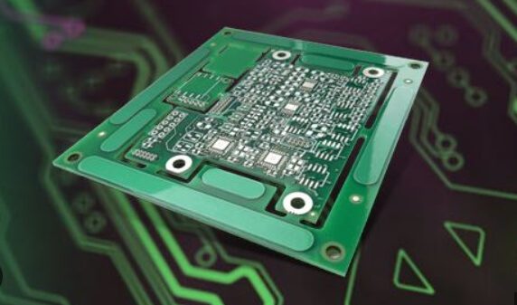
PCB design involves two critical stages: component layout and circuit connection wiring. The layout is the arrangement of circuit components within the PCB’s wiring area. A well-thought-out layout directly affects the ease of subsequent wiring and significantly impacts the PCB’s overall performance. In addition to meeting circuit functionality and performance requirements, a good layout considers manufacturability, inspection, and maintenance. Components should be placed evenly, neatly, and compactly, ensuring that leads and connections are short, minimizing interference and signal transmission delays.

HDI technology in printed circuit boards and other areas has been a critical driver for developing many of the electronics we use today, especially those that have decreased substantially in size and weight in recent years. The smaller the equipment gets, the more likely it is to employ HDI technology
Summary: High-frequency microwave plates should be a new product of high-tech. With the continuous development of communications and computers towards high frequency and high speed, their uses will become wider and wider in the future
Key Takeaways
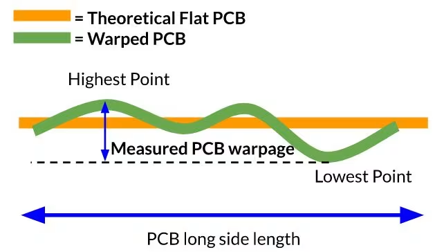
Stress during fabrication, such as thermal expansion and contraction, imbalanced copper distribution, and improper handling, can lead to warpage.
Utilize tools like feeler gauges, height gauges, contour gauges, optical profilometers, and Finite Element Method (FEM) simulations to accurately measure PCB warpage.
Effective design practices using OrCAD X, such as symmetrical component placement and proper copper distribution, combined with precise fabrication controls, can significantly reduce the risk of PCB warpage.
- 1
- 2