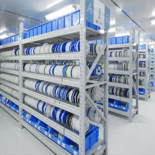
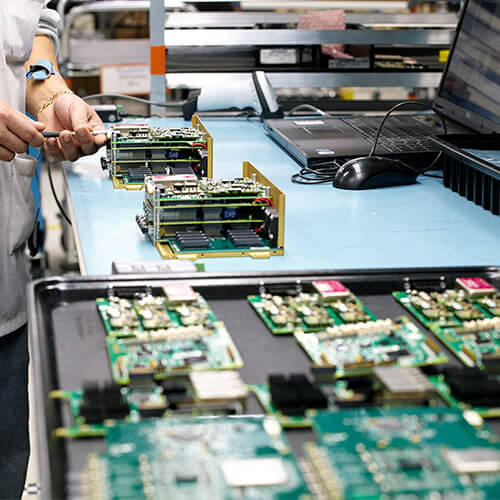
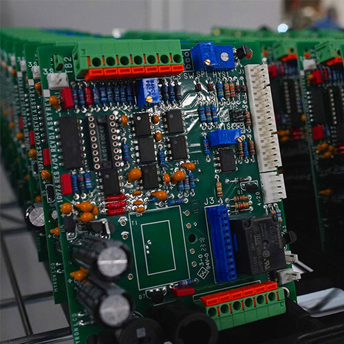
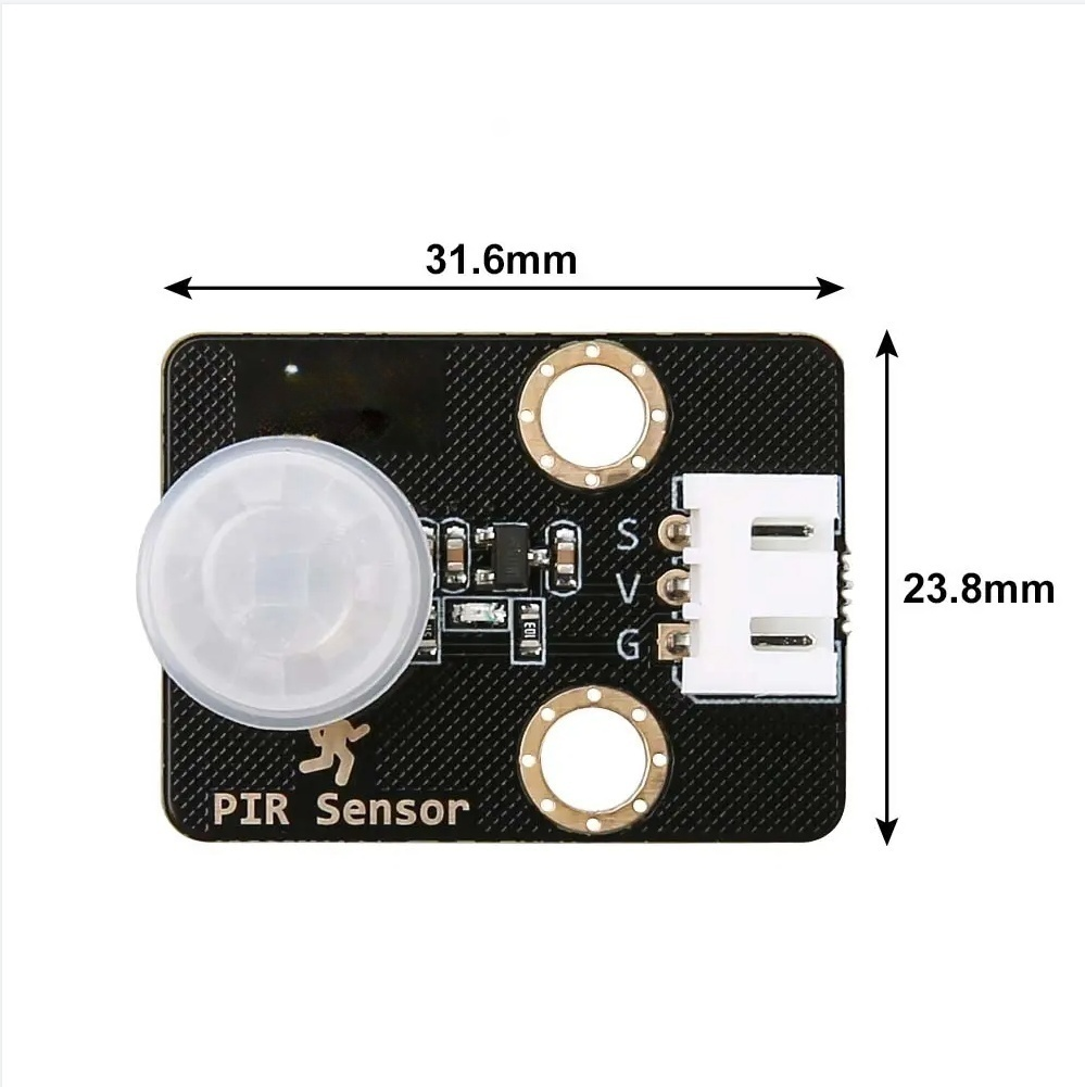
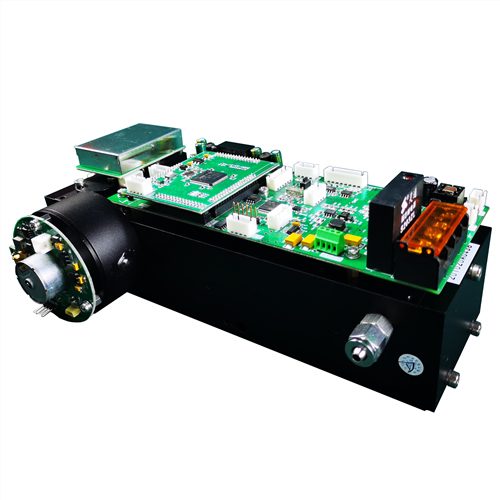
1. Background Overview In industrial automation systems, sensors play a vital role in enabling intelligent monitoring and equipment interaction. A European client recently sought to develop a PIR-based motion sensor module for use in equipment activity detection and control systems. The module required high sensitivity, strong anti-interference capability, low power consumption, and stable performance in […]
1. Background Overview With the growing demand for smart cities and industrial automation, air quality monitoring systems have become critical in factories, laboratories, smart buildings, and underground facilities. A European client developing a gas sensor module for air quality detection required a high-precision, low-power, and stable PCBA solution with strong anti-interference capability. KKPCB was selected […]
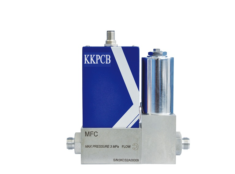
1. Background Overview A European client specializing in industrial automation sought a reliable and high-precision PCBA partner for their mass flow meter product. They needed a solution to improve measurement accuracy, ensure high durability under harsh industrial environments, and maintain competitive cost efficiency. 2. Application Scenario The mass flow meter is widely used in semiconductor […]
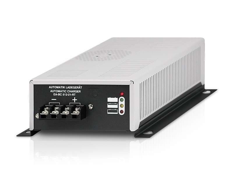
In the field of industrial automation, battery-powered systems have become increasingly important, especially for uninterrupted power supply in mission-critical applications. A European client specializing in compact, high-performance battery chargers for automation systems was seeking a reliable PCBA manufacturing partner to enhance product quality, reduce costs, and improve delivery timelines.
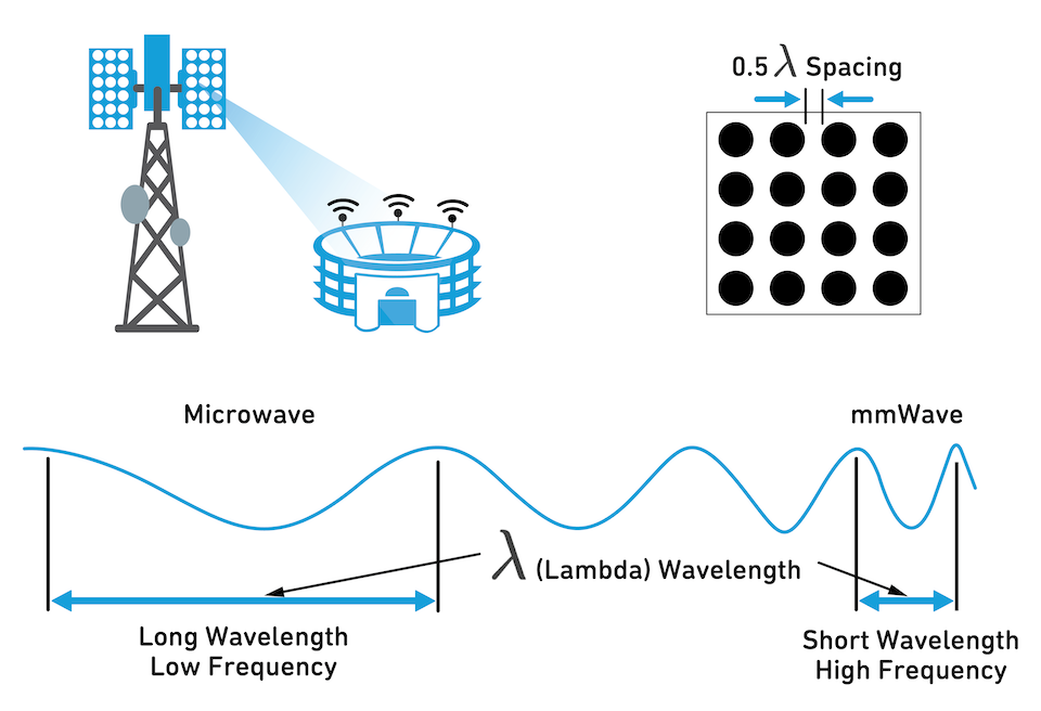
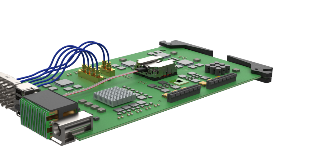
“Enabling Precise Beamforming with Industry-Leading Channel Isolation” Project Overview Customer Background A leading North American 5G infrastructure developer (confidential under NDA) required an advanced 16-transmit/16-receive (16T16R) Massive MIMO antenna array PCB for their next-generation 3.5GHz 5G macro base stations. The design faced critical inter-channel crosstalk issues degrading beamforming accuracy and 3GPP 38.104 compliance. Technical Challenges […]
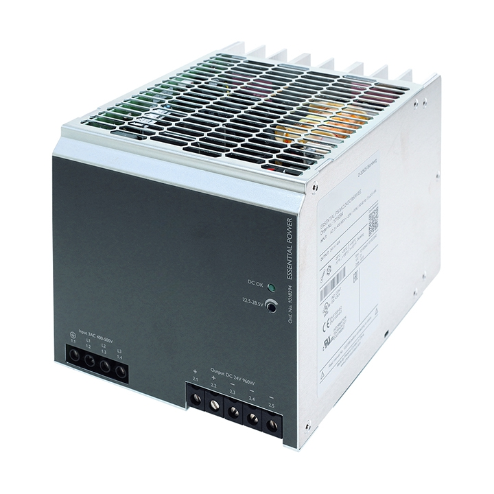
1. Background A European industrial automation customer was developing a power supply module for control systems, requiring high stability, conversion efficiency, and EMC compliance to ensure performance in demanding industrial environments. After evaluating several suppliers, the customer sought a reliable PCBA manufacturer with proven quality control and customization capabilities. 2. Application Scenario The power supply […]
1. Customer Challenge
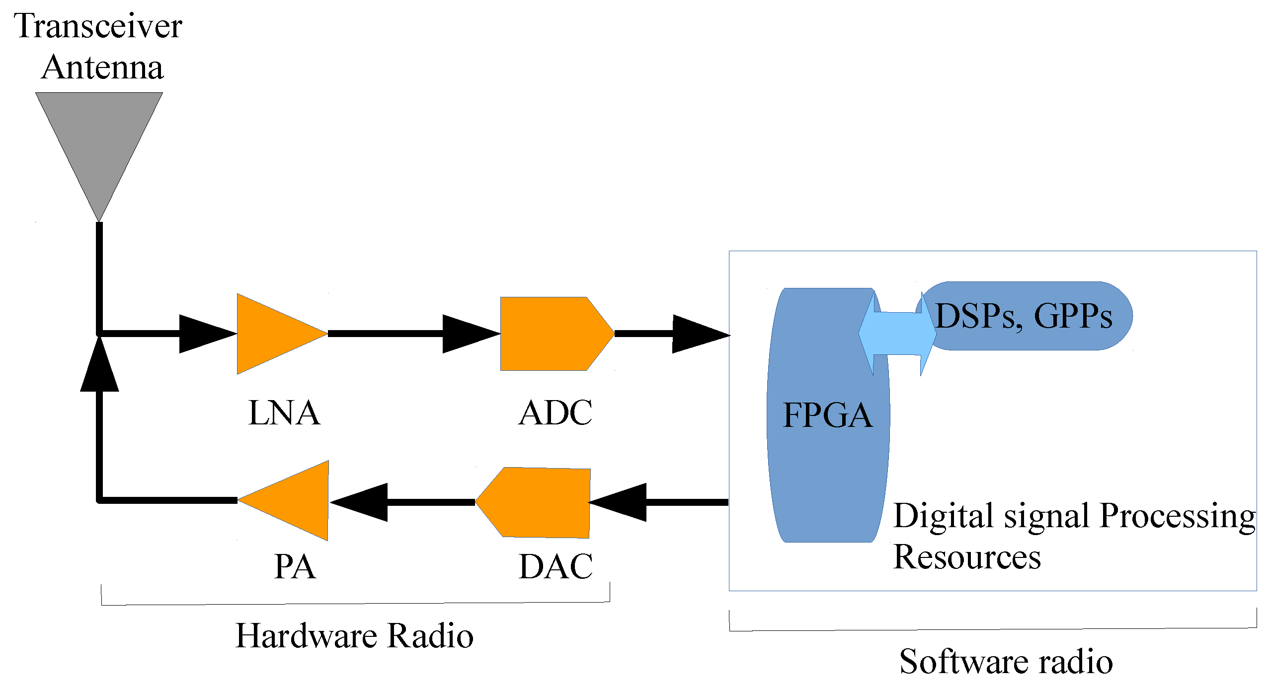
Application: Military/5G Base Station SDR Backplane
Critical Requirements:
Support 12 independent RF channels without interference
Achieve cross-channel isolation >65dB @2.4GHz
Pass FCC Part 90 certification for industrial radio equipment
Withstand harsh environments (85°C/85%RH for 1,000+ hours)
1. Background Overview Under the accelerating global trend of industrial automation, a client from Europe aimed to develop a servo drive product with high dynamic response, high-precision control, and high integration for their next-generation industrial automation equipment. After evaluating multiple suppliers, the client ultimately chose to collaborate with KKPCB, seeking a one-stop customized service from […]
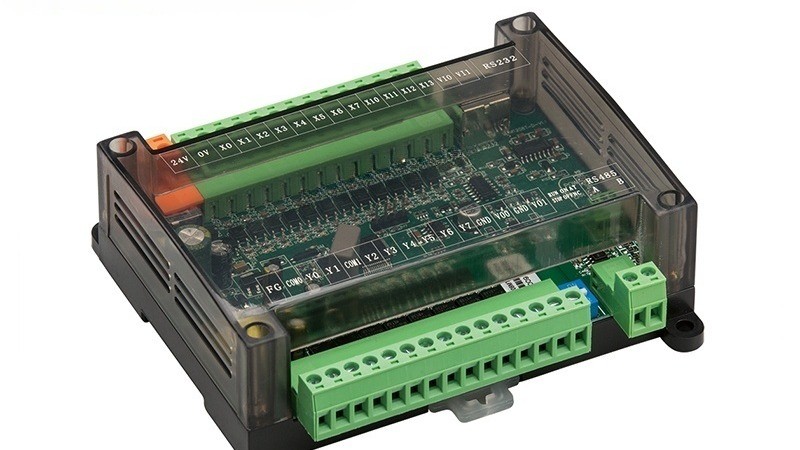
1️⃣ Background Overview With the tightening of global environmental regulations and the upgrading of industrial water resource management needs, sewage treatment plants of customers in Europe, America and the Middle East are in urgent need of highly reliable and extreme environment resistant automation control systems. Traditional PLC modules have pain points such as frequent signal […]
Client: Anonymous
Industry: Fiber Optic Test & Measurement, High-Speed Data Transmission
Application: Next-gen 100G/400G+ optical transceivers, OTDR equipment, and 50GHz RF test modules.
FIS designs precision fiber optic tools, requiring ultra-low-loss PCBs to maintain signal integrity at millimeter-wave frequencies (up to 50GHz). Their challenges include:
Insertion loss degrading high-speed signals (>40Gbps).
Impedance mismatches causing reflection noise.
Thermal expansion leading to microvia cracking in compact designs.


