


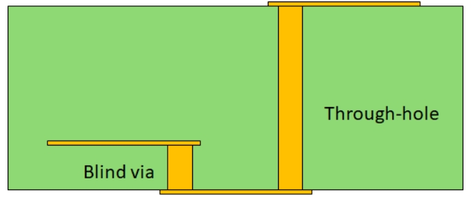
Fabrication capacity for high density PCBs and packaging is currently increasing, especially in North America and Europe. These platforms still use standard via styles, namely through-hole vias, blind and buried vias, and core vias in HDI PCBs. But the electronics assembly and packaging world is no stranger to innovation, and there are alternative via options that can offer much more flexibility in routing and layout.