


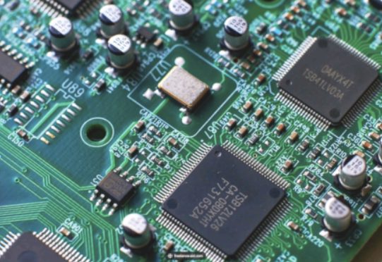
Printed Circuit Board (PCB) routing is a critical aspect of electronic design, ensuring that electrical signals are transmitted efficiently and reliably between components. Proper routing minimizes interference, maintains signal integrity, and meets design requirements such as impedance control and thermal management. This article outlines the best practices for PCB routing, focusing on optimizing performance and ensuring signal integrity.
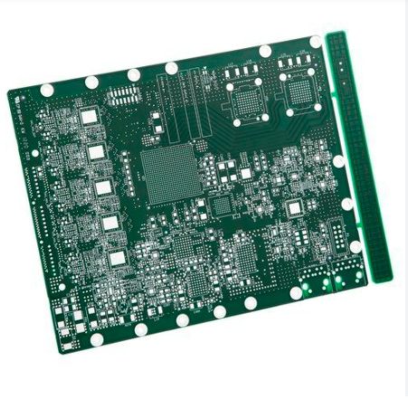
Impedance line routing in multi-layer PCBs is both an art and a science. Adhering to the principles of short lines, symmetry, equal length, and precise compensation ensures high-speed data transmission and robust device performance. By leveraging tools like the Polar Si9000 and applying best practices in design, engineers can effectively address challenges in modern PCB impedance routing.