


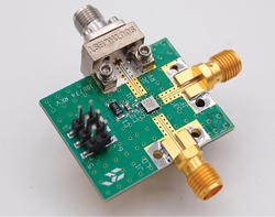
1. Background Overview A European industrial automation client required a compact, high-isolation, and cost-effective magnetic current sensor PCBA to be integrated into their control cabinet systems. The goal was to ensure safe and accurate current monitoring in a high-voltage industrial environment while maintaining stable performance under electromagnetic interference (EMI). 2. Application Scenario The current sensor […]
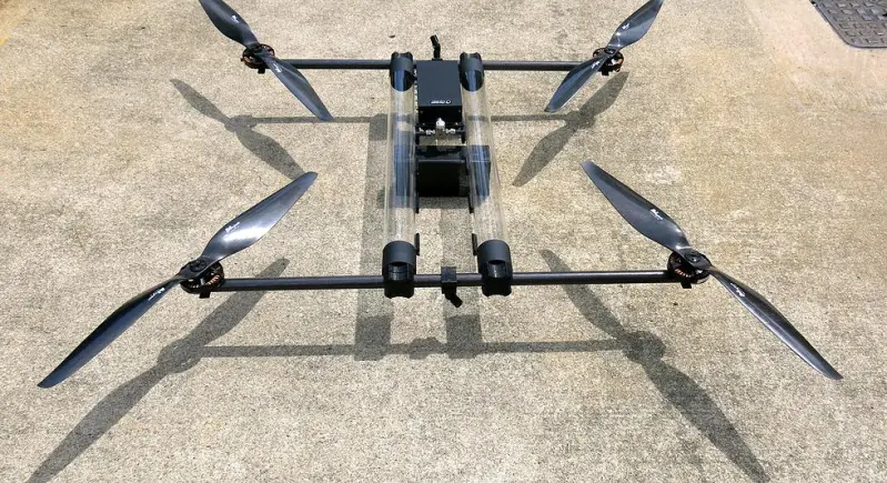
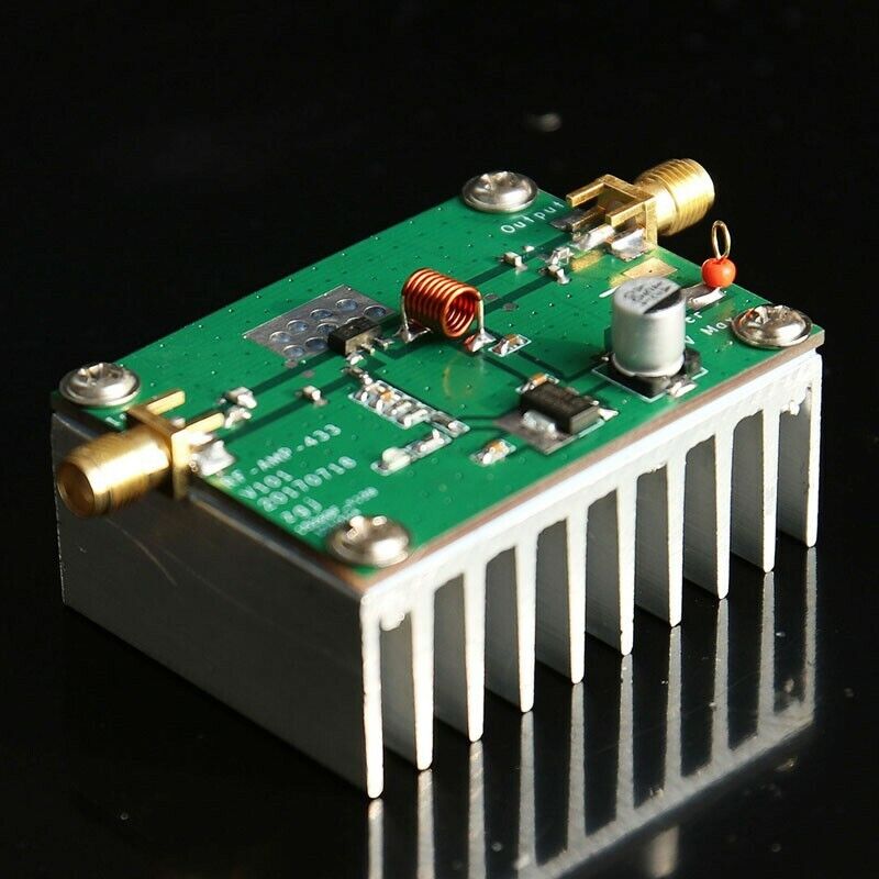
“Reducing Weight by 40% While Maintaining Robustness for Harsh Environment Operations” Project Overview Customer Background A European UAV manufacturer specializing in industrial surveillance (identity protected) required a weight-optimized RF PCBA for their next-generation drone’s communication module, targeting multi-band operation (900MHz/2.4GHz/5.8GHz). The legacy design’s excessive weight (120g) limited flight time, while inadequate environmental protection caused failures […]
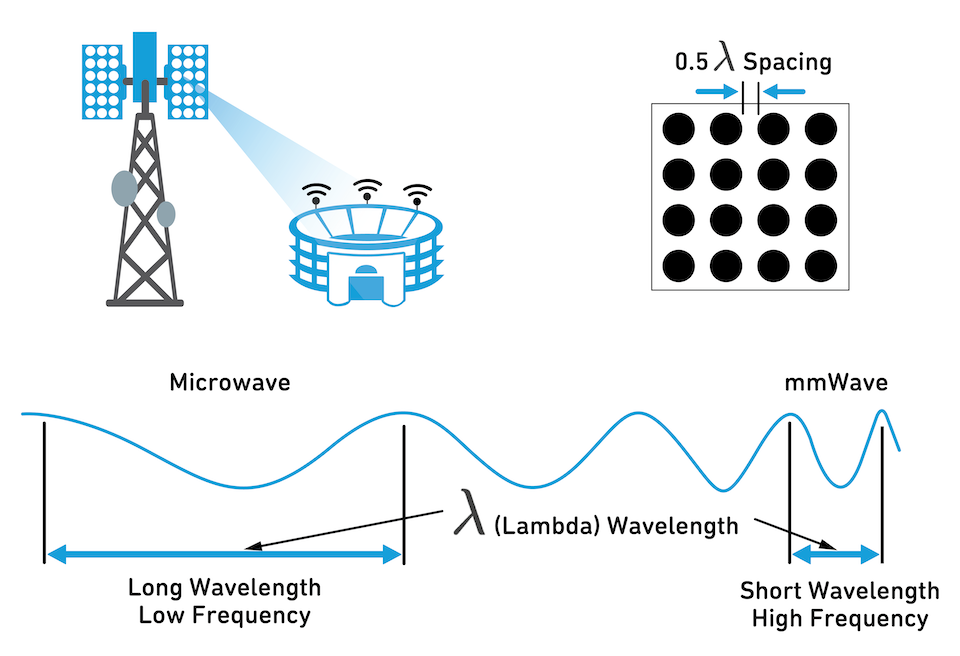
“Enabling Precise Beamforming with Industry-Leading Channel Isolation” Project Overview Customer Background A leading North American 5G infrastructure developer (confidential under NDA) required an advanced 16-transmit/16-receive (16T16R) Massive MIMO antenna array PCB for their next-generation 3.5GHz 5G macro base stations. The design faced critical inter-channel crosstalk issues degrading beamforming accuracy and 3GPP 38.104 compliance. Technical Challenges […]
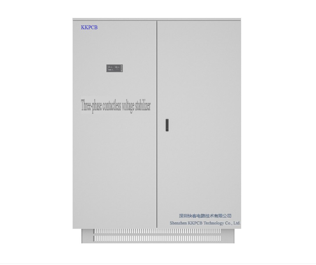
1. Background Overview In modern industrial automation systems, a stable and reliable power supply is critical for ensuring efficient equipment operation. A European client specializing in industrial-grade voltage regulators was seeking to enhance product performance in areas such as voltage stability, thermal control, communication reliability, and cost efficiency. They turned to KKPCB for a customized […]
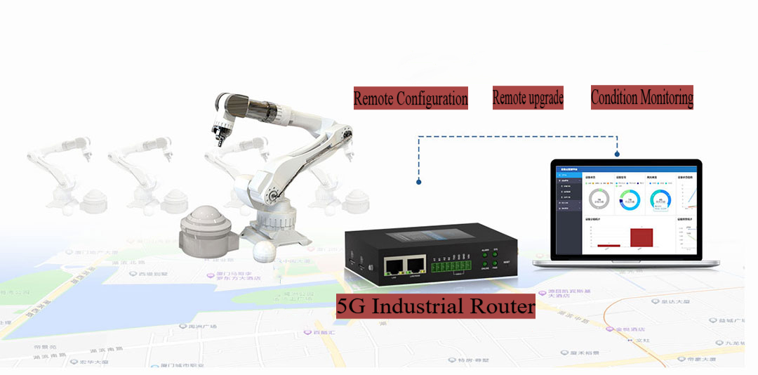
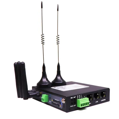
1. Background Overview A European customer in the industrial automation sector required a high-performance and reliable industrial network router for device-to-device communication in their automated systems. The router needed to support high-speed data transfer, strong anti-interference capabilities, remote control functionality, and stable operation in harsh environments. The customer was looking for a supplier with expertise […]
“Enabling Next-Gen LEO Satellite Communication with High-Performance RF PCBs” Project Overview Customer Background A leading European satellite technology provider (identity protected under NDA) required high-reliability PCBs for their next-generation low Earth orbit (LEO) communication terminals, targeting IoT and global broadband connectivity. The system demanded ultra-low-loss signal transmission at Ka-band (26.5-40GHz) to meet ITU-R S.465-6 radiation […]
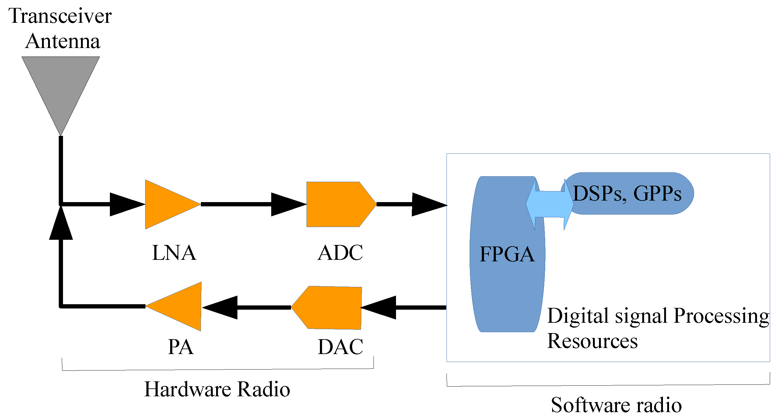
1. Customer Challenge
Application: Military/5G Base Station SDR Backplane
Critical Requirements:
Support 12 independent RF channels without interference
Achieve cross-channel isolation >65dB @2.4GHz
Pass FCC Part 90 certification for industrial radio equipment
Withstand harsh environments (85°C/85%RH for 1,000+ hours)
1. Customer Challenge
Application: 5G Base Station/Radar Power Amplifier
Pain Points:
Low Efficiency: Only 35% at 6GHz, causing excessive heat
Unstable Performance: Return loss > -15dB, signal reflection issues
Material Limitations: FR4-only PCB led to dielectric loss (Df > 0.02 @10GHz)
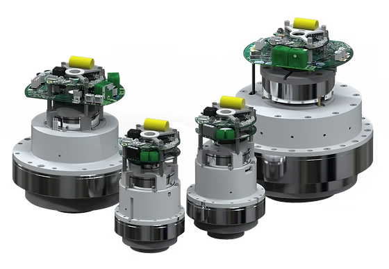
1. Customer Requirements
Application: Industrial robotic joint drive control
Key Challenges:
Integrate 16-channel PWM control + current sampling within 80mm × 60mm
Excessive MOSFET temperature rise (>30°C @20A), causing throttling
Compliance with IEC 61000-6-4 (Industrial EMC Standard)
Client: A Leading Metro System Operator (Asia)Application: Underground Tunnel Communication Systems 1. Operational Challenges Environmental Conditions: Critical Failures Observed:▶ Insulation resistance (IR) dropped to <1GΩ within 6 months▶ Bit Error Rate (BER) surged to 10⁻⁴ (vs. required 10⁻⁸)▶ Frequent corrosion-induced signal loss (3+ annual maintenance interventions) 2. KKPCB’s Robust Manufacturing Solution Core Technical Innovations Technology […]