


1. Background Overview A European customer specializing in voltage regulators was seeking to integrate a new high-performance voltage sensor module into their next-generation products. The client faced challenges such as unstable temperature drift, inefficient component layout, and long delivery cycles. They were looking for a reliable manufacturing partner with strong customization capabilities and ultimately chose […]
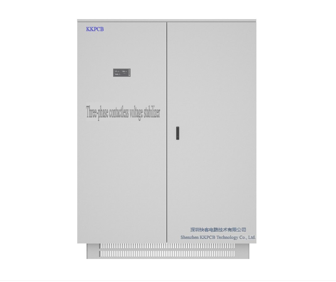
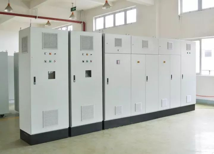
1. Background Overview In modern industrial automation systems, a stable and reliable power supply is critical for ensuring efficient equipment operation. A European client specializing in industrial-grade voltage regulators was seeking to enhance product performance in areas such as voltage stability, thermal control, communication reliability, and cost efficiency. They turned to KKPCB for a customized […]

Industry: Defense Electronics
End Applications:
Armored vehicle main control units
Field communication relay equipment
Manufacturing Challenges:
Heterogeneous material processing (AlSiC metal substrate + FR4 multilayer hybrid lamination)
Extreme environment reliability (MIL-STD-810H vibration compliance)
Military-grade quality control (100% inspection + batch traceability)
Previous Supplier Pain Points:
✔ AlSiC substrate yield only 65% (delamination due to CTE mismatch)
✔ PCIe gold finger contact failure rate 3,000 PPM (post-vibration)
✔ EMP shielding layer vacuum lamination yield below 80%
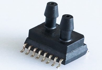
1️⃣ Background Overview Global medical equipment is accelerating its intelligentization, and the requirements for the accuracy and reliability of pressure sensors in ventilators continue to increase. A Middle Eastern medical equipment manufacturer plans to upgrade its ventilator airway control system, which requires a differential pressure sensor module that can operate stably in a high temperature and […]

The customer is a globally leading manufacturer of communication equipment, specializing in the development and production of large-scale routers, switches, servers, and high-speed networking devices. As modern network communications demand increasingly high signal integrity, reliability, and thermal stability, the customer required an 18-layer PCB with low-loss material (S1000-2M) and advanced immersion gold plating to ensure stable signal transmission and long-term reliability
Unlike fixed power supplies that provide a constant output voltage, variable power supplies can be adjusted to different output voltages as needed. In contrast, fixed voltage power supplies or battery chargers provide a single, unchanging output voltage and are designed for specific, consistent power requirements. Read on as we discuss variable power supply PCB layout tips.
PCB layout planning is a critical phase in the design process, enabling engineers to save time and ensure a structured approach to package management, component placement, and routing.
In this article, we’ll dive into the essentials of power integrity, why it matters, and how you can manage it effectively in your PCB designs. Whether you’re new to PCB design or looking to improve your skills, understanding PI is a must for building reliable, high-performance electronics.
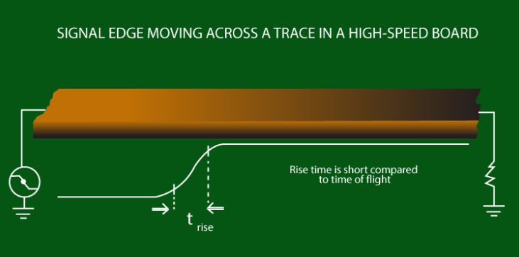
With the continuous development of high-frequency electronic devices, especially in wireless networks and satellite communications, information products are becoming faster and higher in frequency, and communication products are moving towards large capacity and high-speed wireless transmission for voice, video, and data standardization. As a result, the next generation of products requires high-frequency substrates. The process technology for high-frequency PCB production is continuously improving to meet the diverse needs of users. Based on over ten years of experience in PCB production, this article will detail the key technical aspects and considerations for the production of high-frequency microwave PCBs.

Avoiding creep in board assemblies requires a combination of thoughtful design, material selection, and controlled manufacturing processes. Proactively addressing these factors ensures long-term reliability and performance of PCB assemblies, even in demanding environments.