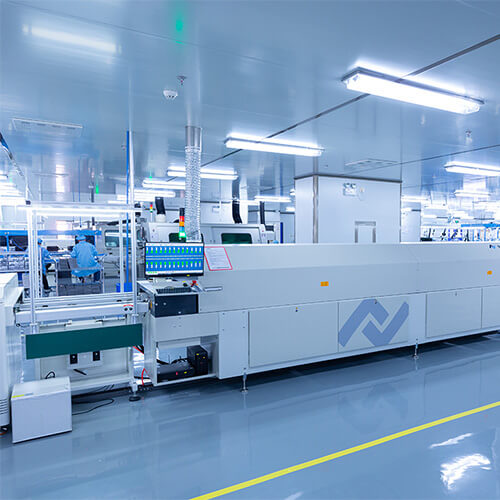
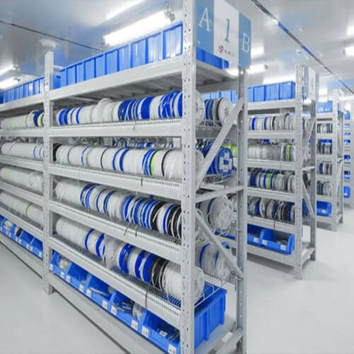
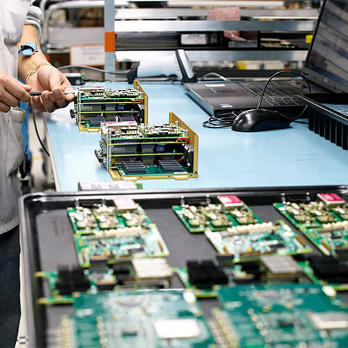
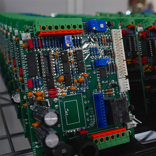
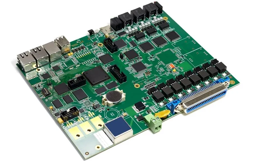
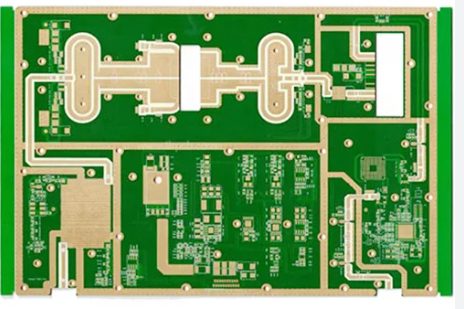
The customer is a globally leading manufacturer of communication equipment, specializing in the development and production of large-scale routers, switches, servers, and high-speed networking devices. As modern network communications demand increasingly high signal integrity, reliability, and thermal stability, the customer required an 18-layer PCB with low-loss material (S1000-2M) and advanced immersion gold plating to ensure stable signal transmission and long-term reliability
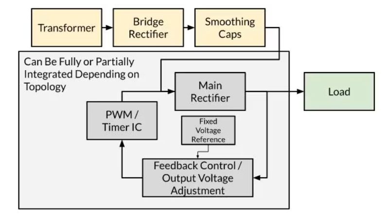
Unlike fixed power supplies that provide a constant output voltage, variable power supplies can be adjusted to different output voltages as needed. In contrast, fixed voltage power supplies or battery chargers provide a single, unchanging output voltage and are designed for specific, consistent power requirements. Read on as we discuss variable power supply PCB layout tips.
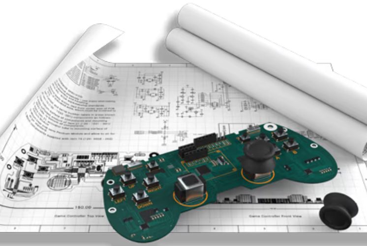
PCB layout planning is a critical phase in the design process, enabling engineers to save time and ensure a structured approach to package management, component placement, and routing.
In this article, we’ll dive into the essentials of power integrity, why it matters, and how you can manage it effectively in your PCB designs. Whether you’re new to PCB design or looking to improve your skills, understanding PI is a must for building reliable, high-performance electronics.
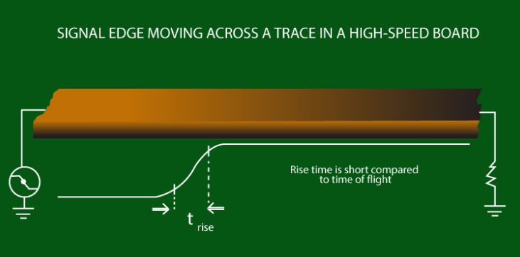
With the continuous development of high-frequency electronic devices, especially in wireless networks and satellite communications, information products are becoming faster and higher in frequency, and communication products are moving towards large capacity and high-speed wireless transmission for voice, video, and data standardization. As a result, the next generation of products requires high-frequency substrates. The process technology for high-frequency PCB production is continuously improving to meet the diverse needs of users. Based on over ten years of experience in PCB production, this article will detail the key technical aspects and considerations for the production of high-frequency microwave PCBs.
Avoiding creep in board assemblies requires a combination of thoughtful design, material selection, and controlled manufacturing processes. Proactively addressing these factors ensures long-term reliability and performance of PCB assemblies, even in demanding environments.
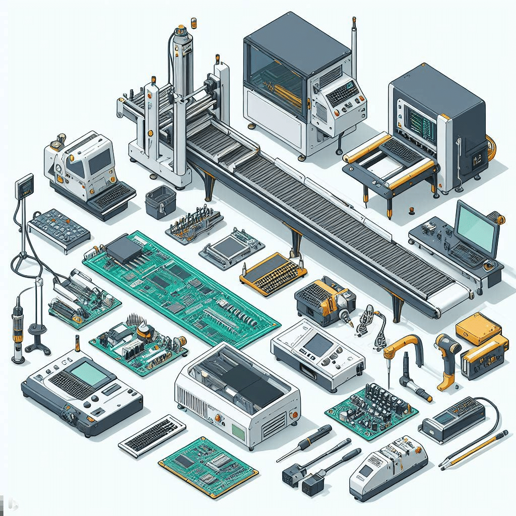
In the world of PCB manufacturing, two main methods are commonly used: PCB prototyping and standard PCB production. Both methods play critical roles and come with their own characteristics. Reducing the time and costs associated with the development process can significantly increase the success rate of future projects. This article explores the benefits of starting with a prototype PCB for design verification before transitioning to standard PCB production assembly.
Designing a high-voltage PCB requires careful planning, adherence to specific guidelines, and a keen eye for safety. Whether you’re working on industrial equipment, power electronics, or consumer devices, the following tips and considerations will ensure you create efficient and safe high-voltage PCB designs.
Solar energy is rapidly gaining popularity as an alternative energy source. One of the key components of a solar energy system is the solar inverter. A solar inverter is a device that converts the direct current generated by solar panels into alternating current
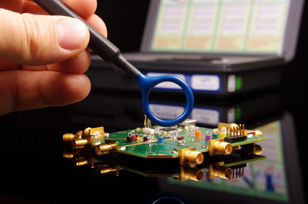
In conclusion, managing EMI and ensuring EMC are critical aspects of PCB design and manufacturing. By carefully considering factors like trace routing, grounding, component selection, and shielding, designers can minimize the risks associated with electromagnetic interference and create devices that perform reliably and safely.


