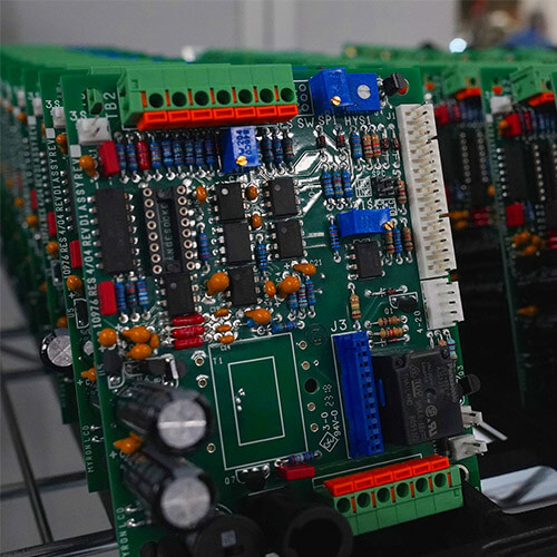
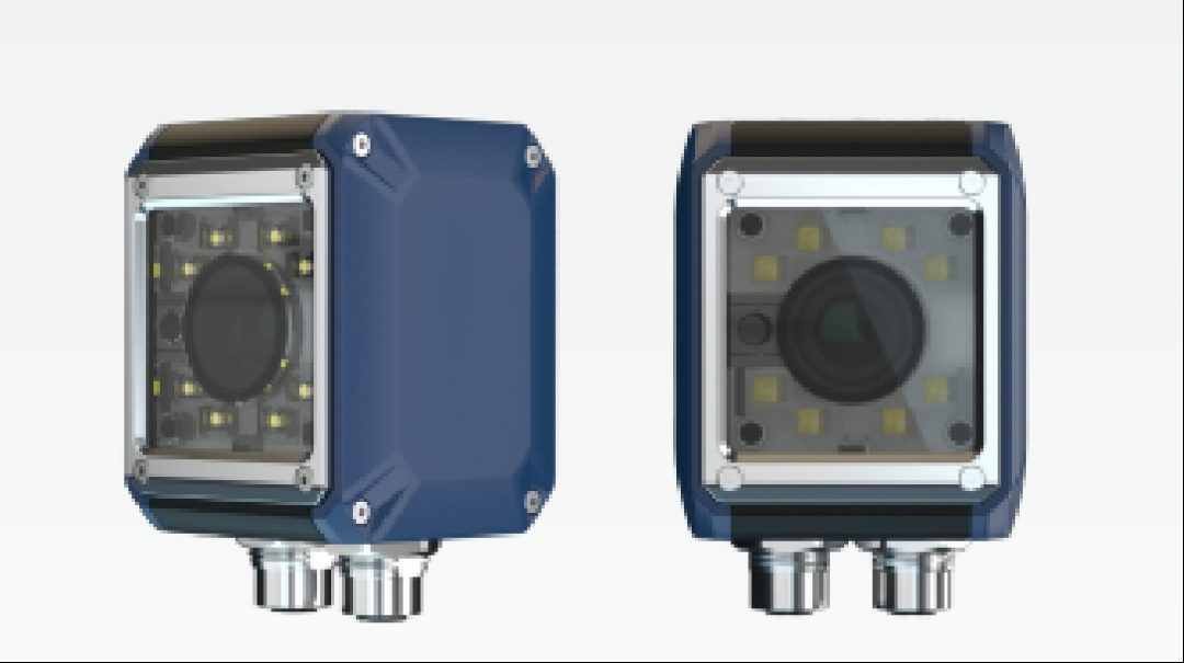
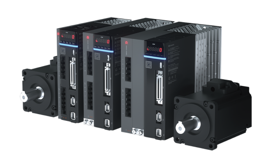
1. Background Overview A European client aimed to develop a high-performance industrial smart sensor for industrial automation systems. The device needed to be compact, highly reliable, and compatible with multiple sensor types, while supporting robust communication protocols and protection mechanisms. To meet their high reliability and mass production consistency requirements, the client partnered with KKPCB […]
Industry Challenges
Legacy System Limitations: 60% of CNC retrofits require motion control upgrades (ABI Research 2024)
Precision Demands: PCB drilling needs ±5μm positioning accuracy at 120IPM
Cost Pressure: Traditional solutions exceed $3k/axis
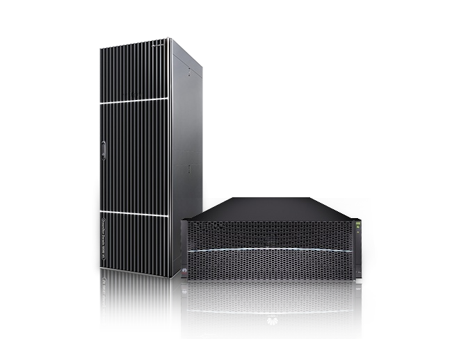
1. Background Overview With the rising demand for data processing and real-time analysis in industrial automation systems, high-speed and reliable data storage devices have become essential. A European industrial equipment manufacturer approached KKPCB for a customized PCBA solution for their new-generation data storage modules. The goal was to ensure high performance, reliability, and cost-efficiency under […]
Industry Challenges in Thermal Testing
Measurement Complexity: 73% of electronic component failures originate from thermal stress (IEEE Reliability Report)
Channel Limitations: Conventional systems max out at 64 channels with 1.5°C accuracy
Data Integration: 68% testing time wasted on multi-instrument synchronization
I. Innovation Background
Market Pain Points
Battery Dependency: 78% of wireless doorbell failures caused by battery issues (Consumer Reports 2023)
Installation Limitations: Wired solutions require complex retrofitting
Range Reliability: Typical products fail beyond 30m/2 walls
I. Strategic Market Positioning
Industry Pain Points
Limitations of Traditional Interfaces: 62% of Industrial Operators Express Frustration with Outdated HMI Systems (ABI Research 2024)
Multi-Platform Integration: Growing Demand for Unified Control across IoT/Operational Technology (OT) Systems
Safety Compliance: EN 61000-6-2/-4 Standards Become Mandatory for Industrial HMI
KKPCB’s power electronics solutions address critical needs in:Collaborative robot joint control,Mobile robot battery management,Precision motion systems
“KKPCB’s hardware reliability was crucial for our 99.3% field uptime. Their agricultural PCB expertise is unmatched.”
— Client CTO
KKPCB’s full-spectrum solution helped us build a technical moat in eye protection – this is true differentiated innovation
Customer Requirements
A smart home manufacturer planned to develop a high-end smart door lock with the following core requirements

