


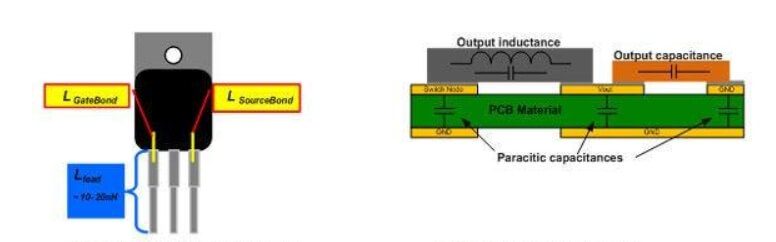
Based on recent trends, improving efficiency is a key goal, and the trade-off of using slow switching devices for better EMI is not worth it. Superjunctions can improve efficiency in applications where planar MOSFETs struggle. Superjunction MOSFETs significantly reduce on-resistance and parasitic capacitance compared to traditional planar MOSFET technology. The significant reduction in on-resistance and reduced parasitic capacitance, while helping to improve efficiency, also produces fast switching transitions of voltage (dv/dt) and current (di/dt), forming high-frequency noise and radiated EMI.
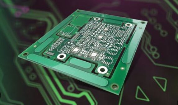
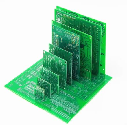
In today’s technology-driven world, the Printed Circuit Board (PCB) stands as a foundational component in electronic devices. From smartphones to complex medical equipment, PCBs are essential for ensuring reliable electrical connections and functionality. This article delves into the critical stages of PCB design, manufacturing, and final artwork, providing insights into the complexities and technicalities of creating effective circuit boards.
Addressing signal integrity (SI) issues early in the PCB design process can streamline the design and eliminate the need for corrective termination devices later. Here, we outline critical steps to maintain signal integrity, from planning through testing.

Mastering these PCB design rules—like efficient grounding, proper trace sizing, and capacitor placement—significantly improves design quality and efficiency. By following these guidelines, you can reduce rework, save costs, and achieve more reliable, higher-quality PCB designs
Following these practical tips for high-frequency PCB design helps in optimizing interconnections within the board. Techniques such as using 45° transmission lines, precision etching, and non-leaded components will significantly enhance circuit performance. Familiarizing yourself with these methods makes designs like back-copper coplanar microstrip layouts both economical and efficient.
Proper PCB design requires careful planning and attention to detail, from schematic creation to component layout and wiring. Following these best practices ensures optimized signal integrity, reduces interference, and minimizes manufacturing issues, leading to higher-quality and more reliable PCB designs.
Understanding these common misunderstandings in circuit design is essential for engineers who want to improve efficiency, reduce power consumption, and design more reliable systems. By addressing these myths, you can avoid co
Electromagnetic compatibility (EMC) refers to the ability of electronic devices to function harmoniously in their electromagnetic environment without causing or being affected by electromagnetic interference (EMI). The goal of EMC design is to enable electronic devices to resist external interference while minimizing the electromagnetic interference they emit to surrounding devices
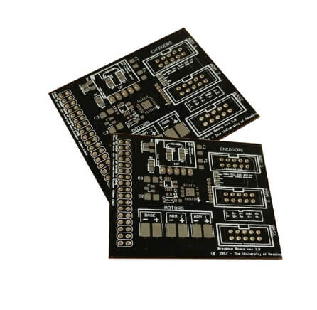
PCB design involves two critical stages: component layout and circuit connection wiring. The layout is the arrangement of circuit components within the PCB’s wiring area. A well-thought-out layout directly affects the ease of subsequent wiring and significantly impacts the PCB’s overall performance. In addition to meeting circuit functionality and performance requirements, a good layout considers manufacturability, inspection, and maintenance. Components should be placed evenly, neatly, and compactly, ensuring that leads and connections are short, minimizing interference and signal transmission delays.
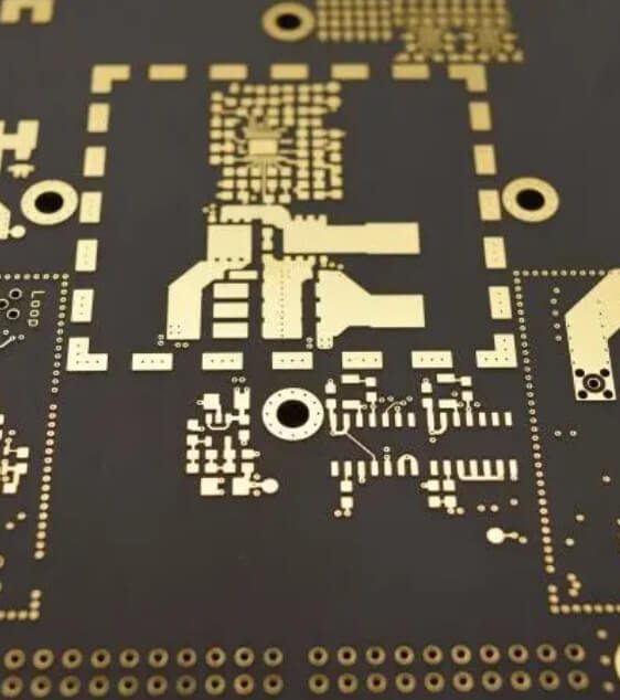
RF and microwave signals are very sensitive to noise -much more sensitive than high -speed digital signals. This means that you need to minimize the noise, bell, and reflection, and at the same time be careful to deal with the entire system.
Returning the signal with the least inductance -the ground floor below the signal will be easier to ensure this path.
Discipline matching is important. With the rise of RF and microwave frequency, the tolerance will become smaller. Generally, the PCB drive needs to be fixed, such as 50 ohms, which means that during the transmission and sending to the receiver, the drive outputs 50 ohms.
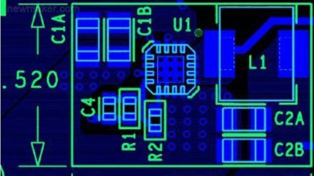
The transmission line that is curved due to wiring restrictions should use a curved radius that is at least three times larger than the central conductor width. This will minimize characteristic impedance.
It is necessary to minimize the return loss, whether it is reflected by the signal or the bell. There will always be a return path, but your design should guide it and prevent the return from multi -layer leakage through the PCB.