


Special processing technologies are non-conventional processes used in the production of printed circuit boards to meet specific needs. These technologies usually involve high-precision, high-complexity processing requirements and are capable of processing circuit boards with special functions or properties, such as high-frequency PCBs, flexible PCBs, and high-density interconnect (HDI) boards.
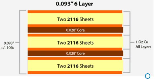
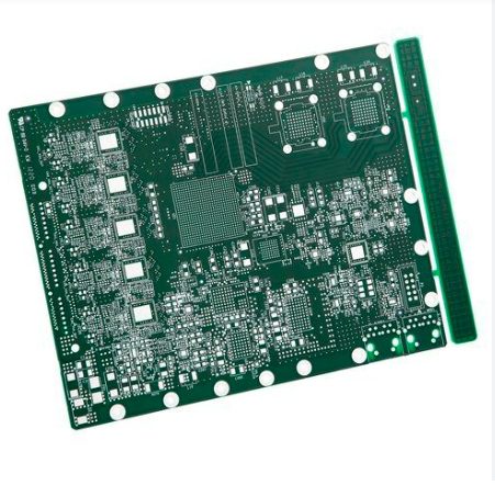
Printed circuit boards (PCBs) have evolved from simple single or double layer boards to complex multilayer boards with 6 or more layers to accommodate increasing component density and interconnectivity needs. 6 layer PCBs provide more flexibility for routing, plane separation and enable partitioning of circuits across layers.
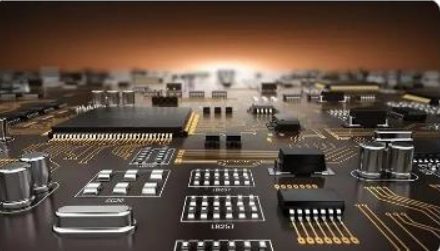
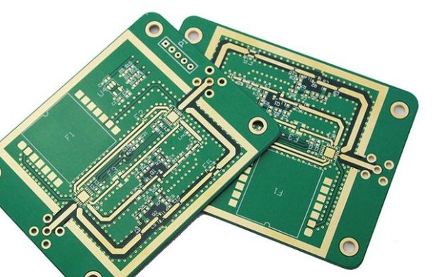
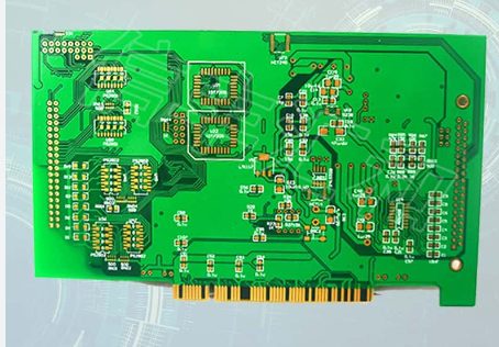
Circuit boards play a key role in making sure electronic products work properly. They provide structural support and link all the electrical parts together. Whether it’s in smartphones, laptops, or household devices, none could operate without a PCB
PCB design requires understanding physical processes and careful organization of layers, power networks, and signal paths. Following these recommendations reduces noise risk, improves reliability, and simplifies the routing of complex systems
Impedance line routing in multi-layer PCBs is both an art and a science. Adhering to the principles of short lines, symmetry, equal length, and precise compensation ensures high-speed data transmission and robust device performance. By leveraging tools like the Polar Si9000 and applying best practices in design, engineers can effectively address challenges in modern PCB impedance routing.
Closely spaced vias are a common design challenge in multi-layer and high-speed PCB boards. Understanding the implications of tight spacing—such as drilling process inefficiencies, reduced solder ring size, and long-term reliability concerns—is essential. By adhering to recommended spacing guidelines, optimizing via placement, and collaborating with manufacturers, designers can enhance production yield, reduce costs, and ensure robust product per
Addressing power supply noise interference in PCB design involves a systematic approach to layout optimization, filtering, and grounding. By understanding the root causes of power supply noise and applying the countermeasures outlined above, designers can significantly enhance circuit performance and reliability. A clean power supply, well-isolated signal paths, and proper filtering are key to achieving a noise-resilient PCB.
Incorporating schematic simulation into the PCB design process not only saves valuable time but also increases the accuracy and efficiency of the entire workflow. By automating the process of checking for errors and verifying connections, designers can improve the overall quality of the PCB and minimize the chances of issues in the final design.
When applied correctly, copper coating offers more benefits than drawbacks, providing improved performance, noise reduction, and thermal management for PCBs. However, to achieve the best results, it’s crucial to carefully consider the design, including grounding, copper areas, and the specific requirements of high-frequency or low-frequency circuits. By paying attention to these details, designers can optimize the copper coating for better overall performance.
Impedance plays a critical role in the functionality, reliability, and performance of printed circuit boards (PCBs). Understanding and managing impedance is essential for ensuring proper signal transmission and maintaining the integrity of the electronic devices that rely on these boards. Below is a detailed analysis of impedance and its importance in PCB design and manufacturing.