


As electronic devices become increasingly miniaturized, advancements in component and wiring technologies have created new challenges for production testing. Highly integrated ICs, smaller insulation spacings, and limited access to circuit nodes have made traditional testing methods insufficient. To address these challenges, a design-for-testability (DFT) approach is essential to reduce testing costs and enhance production efficiency. This guide explores the principles, strategies, and best practices for improving PCB testability.
Achieving efficient automatic PCB wiring involves a blend of strategic planning, tool utilization, and manual refinement. By setting robust design rules, optimizing layout, and leveraging EDA tools effectively, engineers can create high-quality PCB designs that meet performance and manufacturability requirements. The iterative approach of routing, validating, and refining ensures that even the most complex designs achieve high routing rates and functionality.
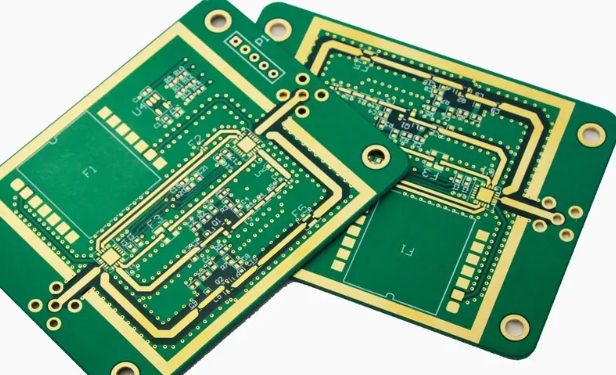
RF (Radio Frequency) circuits and interfaces exhibit unique characteristics, requiring specialized design considerations. These challenges are due to the nature of RF signals and their interaction with physical elements of the circuit. Understanding these aspects ensures optimal performance in wireless communication systems. Below is an exploration of RF circuit characteristics, PCB design considerations, and optimization techniques.
Grounding is a critical aspect of PCB design, particularly in mixed-signal environments where digital and analog circuits coexist. Proper grounding ensures stable performance, minimizes noise, and improves the reliability of the overall circuit. Below are key insights and guidelines to address grounding challenges effectively.
In power supply design, PCB layout plays a critical role in ensuring the circuit’s efficiency, stability, and reliability. Below are five essential considerations for effective PCB design in power supply applications:
This guide delves into the four fundamental characteristics of RF circuits—RF interface, small desired signals, large interference signals, and adjacent channel interference—and highlights essential considerations for PCB design.
Train personnel to consistently cut boards following the structural texture direction. If size variation persists, consider alternative substrate materials.
Work with laminate manufacturers to determine proper stress-relief processes before production.
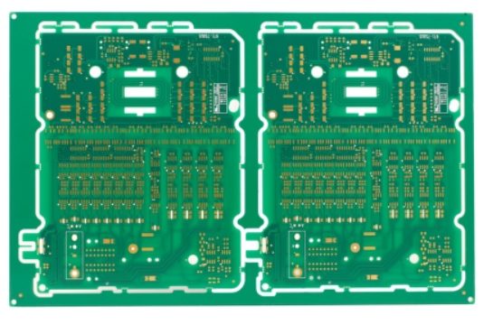
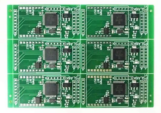
Design for Manufacturability (DFM) optimizes designs for the manufacturing process, making it an essential component of concurrent engineering. By considering factors such as manufacturability and assembly requirements early in the design phase, DFM streamlines production, bridges CAD-CAM communication, and enhances product reliability. Here, we cover general technical requirements for DFM in PCB manufacturing.
Recently, I have been conducting ESD (Electro-Static Discharge) testing on various electronic products. From the test results, I realized that ESD is crucial: if the PCB design lacks proper ESD protection, static electricity can cause devices to freeze or even damage their components. Previously, I only understood that ESD could damage individual components, but now I see the importance of giving full attention to ESD protection throughout the entire design process.
Four-layer PCBs are typically used for high-density, high-frequency applications and offer more than 20 dB better electromagnetic compatibility (EMC) compared to two-layer boards. In a four-layer board setup, a complete ground plane and a full power plane can be used. This allows the various circuit ground wires to be connected to the ground plane effectively, with working noise managed separately.