


PCB interconnections can be categorized into three main types: chip-to-PCB, interconnections within the PCB, and PCB-to-external devices. High-frequency PCB designs require addressing RF effects at these interconnection points to ensure optimal performance. This guide covers techniques for minimizing RF interference, crosstalk, and return loss across these interconnection types.
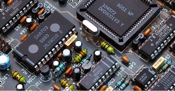
Printed circuit boards (PCBs) remain the backbone of electronic assembly across various systems. Even with perfectly designed schematics, poor PCB design can significantly compromise reliability. For instance, closely spaced thin parallel lines on a PCB can cause signal waveform delays and reflected noise at transmission line terminals. This guide outlines essential considerations for designing reliable PCBs.
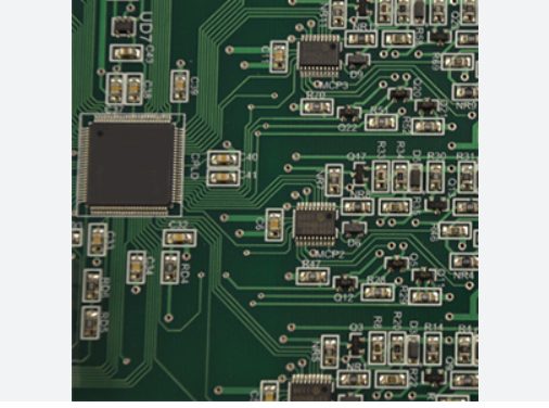
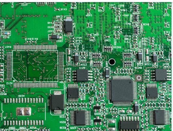
As electronic devices become increasingly miniaturized, advancements in component and wiring technologies have created new challenges for production testing. Highly integrated ICs, smaller insulation spacings, and limited access to circuit nodes have made traditional testing methods insufficient. To address these challenges, a design-for-testability (DFT) approach is essential to reduce testing costs and enhance production efficiency. This guide explores the principles, strategies, and best practices for improving PCB testability.
Achieving efficient automatic PCB wiring involves a blend of strategic planning, tool utilization, and manual refinement. By setting robust design rules, optimizing layout, and leveraging EDA tools effectively, engineers can create high-quality PCB designs that meet performance and manufacturability requirements. The iterative approach of routing, validating, and refining ensures that even the most complex designs achieve high routing rates and functionality.
RF (Radio Frequency) circuits and interfaces exhibit unique characteristics, requiring specialized design considerations. These challenges are due to the nature of RF signals and their interaction with physical elements of the circuit. Understanding these aspects ensures optimal performance in wireless communication systems. Below is an exploration of RF circuit characteristics, PCB design considerations, and optimization techniques.
Grounding is a critical aspect of PCB design, particularly in mixed-signal environments where digital and analog circuits coexist. Proper grounding ensures stable performance, minimizes noise, and improves the reliability of the overall circuit. Below are key insights and guidelines to address grounding challenges effectively.
In power supply design, PCB layout plays a critical role in ensuring the circuit’s efficiency, stability, and reliability. Below are five essential considerations for effective PCB design in power supply applications:
This guide delves into the four fundamental characteristics of RF circuits—RF interface, small desired signals, large interference signals, and adjacent channel interference—and highlights essential considerations for PCB design.
Train personnel to consistently cut boards following the structural texture direction. If size variation persists, consider alternative substrate materials.
Work with laminate manufacturers to determine proper stress-relief processes before production.
Design for Manufacturability (DFM) optimizes designs for the manufacturing process, making it an essential component of concurrent engineering. By considering factors such as manufacturability and assembly requirements early in the design phase, DFM streamlines production, bridges CAD-CAM communication, and enhances product reliability. Here, we cover general technical requirements for DFM in PCB manufacturing.