


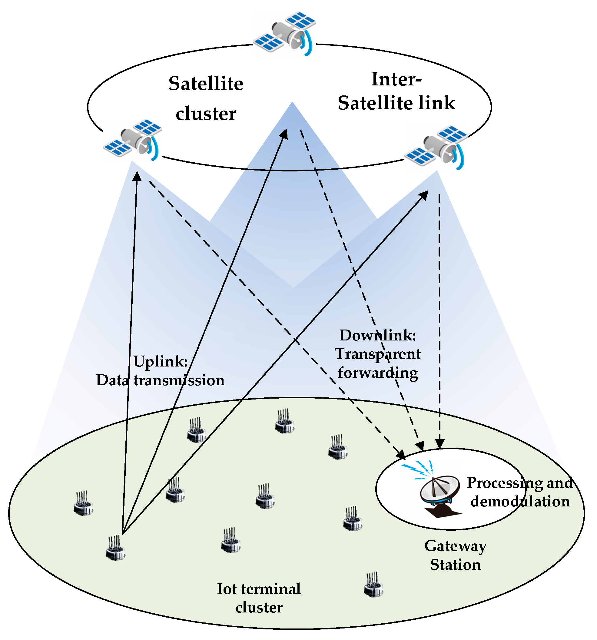
(ASTM E1647 Validated, 60% Cost Reduction vs. Ceramic Substrates) Project Introduction This project developed a mission-critical PCB for commercial satellite IoT terminals requiring: “The Rogers/Taconic hybrid stackup solved our insertion loss and CTE mismatch problems simultaneously.”— Lead RF Engineer (Client R&D Team) Key Specifications Parameter Target Achieved Frequency Range 902-928MHz (LoRa) + 1.5GHz (SatIoT) 850MHz-1.6GHz […]
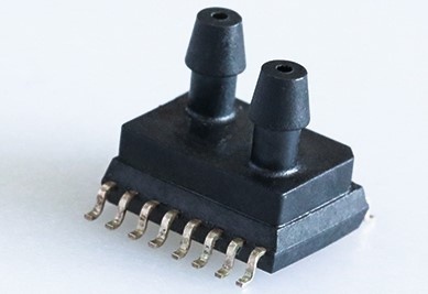
1️⃣ Background Overview Global medical equipment is accelerating its intelligentization, and the requirements for the accuracy and reliability of pressure sensors in ventilators continue to increase. A Middle Eastern medical equipment manufacturer plans to upgrade its ventilator airway control system, which requires a differential pressure sensor module that can operate stably in a high temperature and […]
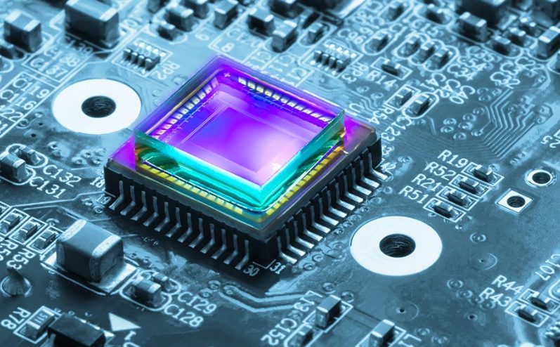
Sensors and transducers play integral roles in PCBs by enabling electronic systems to interact with and respond to the surrounding environment. Sensors detect physical parameters such as temperature, pressure, light, and motion, converting these analog signals into electrical signals that PCBs process. Sensors are used in various applications, from environmental monitoring and industrial automation to consumer electronics.
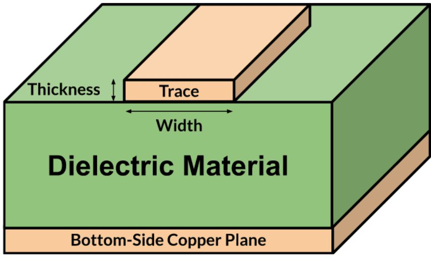
The relationship between PCB trace thickness and current capacity is a critical aspect of PCB design. Properly sizing traces ensures that they can handle the required current without overheating, which is essential for the reliability and functionality of the circuit. This article explores the key considerations for selecting trace thickness, the impact of copper weight, and methods for calculating current capacity, along with design strategies for high-current applications
Creating a robust component library is one of the most challenging yet critical aspects of PCB design. The quality of the library, which includes schematic symbols, PCB footprints, and 3D models, directly impacts the success of your board development. Among these, the PCB footprint plays a pivotal role in determining whether your board can be manufactured and assembled correctly.
Low power circuit design includes strategies focused on minimizing both dynamic and static power usage in your printed circuit boards. While selecting components with low power requirements is a crucial element, low power PCB design involves more comprehensive considerations to effectively manage power consumption.

Military and aerospace PCBs must adhere to intensely high standards to ensure their safety and functionality in the extreme conditions they’re used in. For this reason, PCB design for military and aerospace applications requires incredibly stringent guidelines with built in redundancy, extra safety, and stringent tolerances, minimizing risk of failure
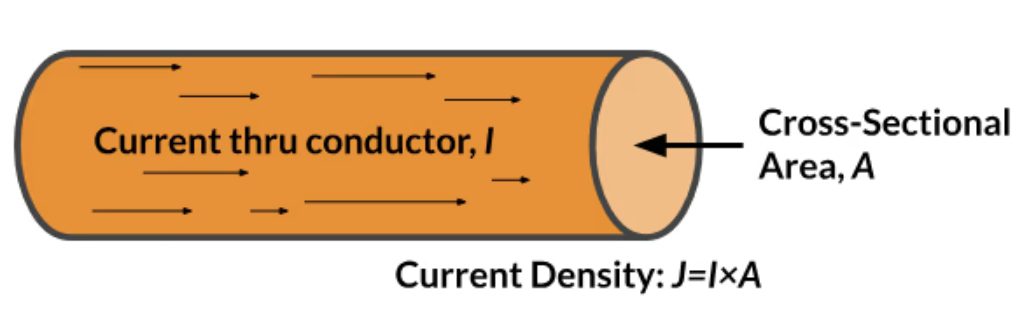
Copper current density refers to the amount of continuous current going through a copper wire —whether on a circuit board as a trace or not. According to the principles of Joule or Ohmic heating (represented as VI or I²R), any material that conducts electricity will generate heat, leading to a gradual rise in temperature in both the conductor and its surrounding environment.
When designing a printed circuit board (PCB), engineers often focus on ensuring the correct impedance structures and electrical performance of the board. However, the physical characteristics, such as PCB thickness, are equally important and can significantly impact the cost, manufacturability, and performance of the final product. While standard PCB thicknesses are widely used, they are more of a convention than a strict requirement, offering designers an opportunity for optimization, especially in high-volume production.
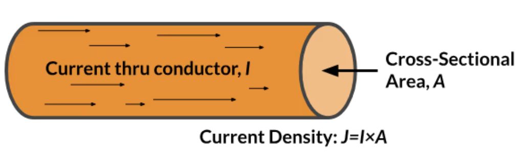
According to Joule or Ohmic heating principles (represented as VI or I²R), any conductive material generates heat, leading to a gradual temperature rise in both the conductor and its surroundings. Managing copper current density is critical to ensure reliable PCB performance and prevent overheating. This article explores key considerations, design guidelines, and tools like OrCAD X to optimize copper current density in PCB designs.