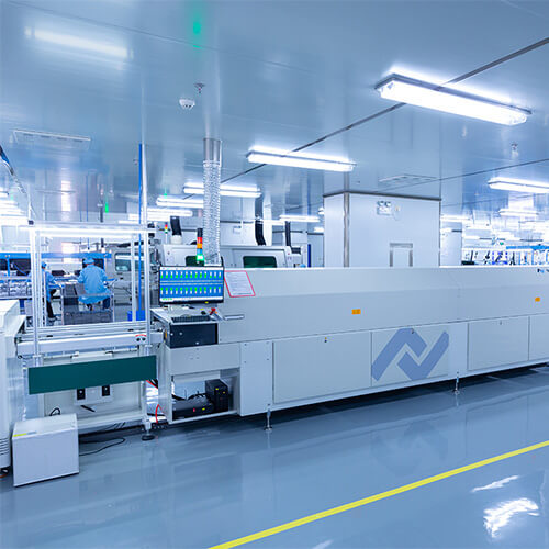
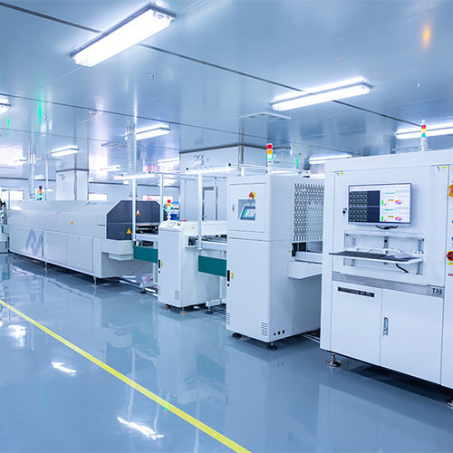
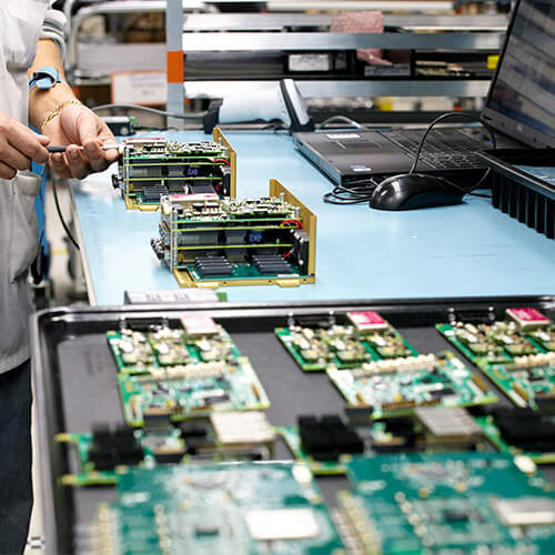
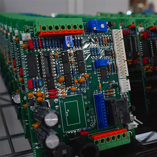
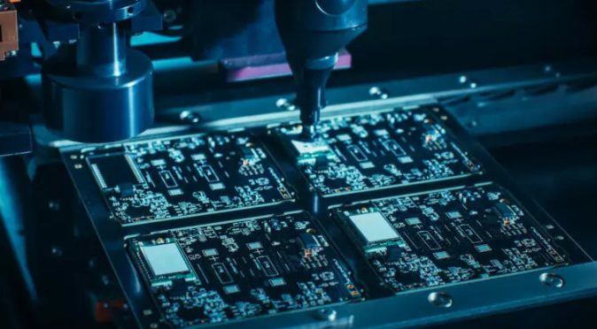
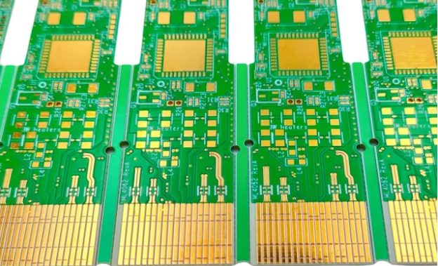
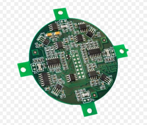
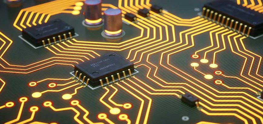
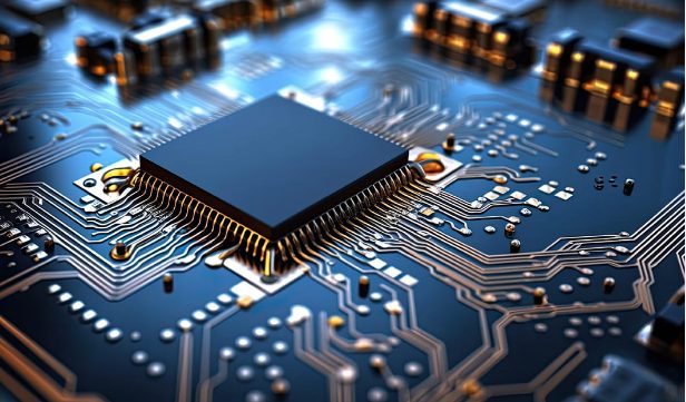
When assembling a printed circuit board (PCB), components are mounted onto the board through one of two primary methods: Surface Mount Technology (SMT) or Through-Hole Technology (THT). Each method has distinct advantages and is suited to different applications depending on the project requirements.
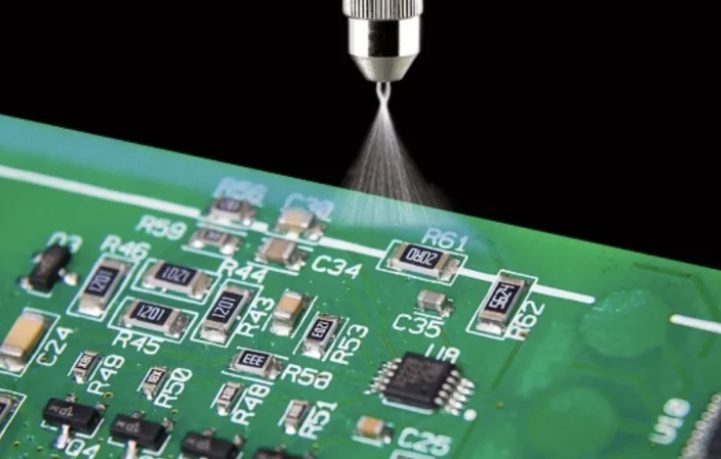
Conformal coatings play a critical role in ensuring the longevity and reliability of printed circuit boards (PCBs). Whether designing electronics for consumer devices, automotive systems, or military applications, selecting the right conformal coating is essential.
In this article, we’ll dive into the essentials of power integrity, why it matters, and how you can manage it effectively in your PCB designs. Whether you’re new to PCB design or looking to improve your skills, understanding PI is a must for building reliable, high-performance electronics.
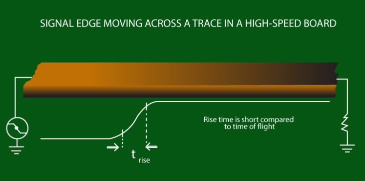
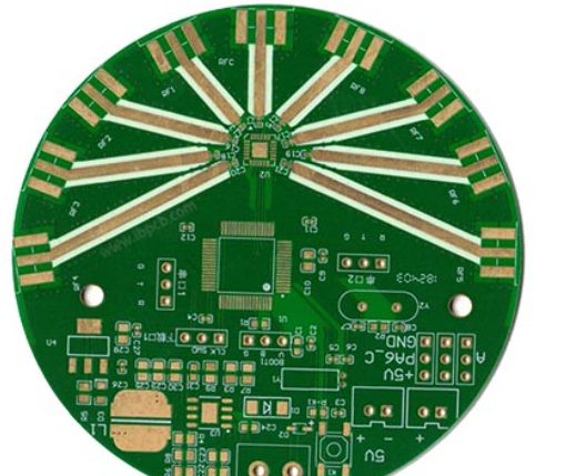
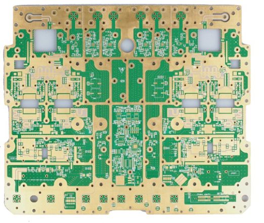
High frequency PCBs are specialized circuit boards designed to transmit signals over a gigahertz (GHz) frequency range, ensuring quick and reliable communication in devices ranging from military radar systems to smartphones.
In recent years, electronic products have become increasingly complex and integrated into people’s daily lives. However, there are still two popular methods for soldering electronic components together to build circuits:
Surface Mount Technology (SMT) for PCB Assembly
Through-Hole (PTH) PCB Assembly
Thermostats are an essential part of our daily lives and industrial systems, regulating temperature to maintain stable conditions in both equipment and environments. However, to ensure thermostats operate reliably under various conditions, the core technology behind them—PCB (Printed Circuit Board) design—must meet high standards. This article explores the key factors to consider when designing a thermostat PCB and how to ensure its efficient and reliable performance.
These outstanding characteristics of coated and resin PCBs emphasize the necessity of analyzing the system and requirements to make the right decision. Coatings have different functions and disadvantages. The same is true for resin PCBs. To complicate matters, some devices now adopt 2K coated PCBs due to their advanced characteristics.
The PCB design industry is one of the world’s leading industries. As the world develops, the importance of the PCB industry seems likely to continue to grow for the foreseeable future. Learning how to manage and track the heat of PCBs is essential to gaining widespread potential in related markets and achieving high-temperature PCBs
High-Frequency PCB is a subcategory in the field of PCB that is designed with extremely high electromagnetic frequencies. The typical frequency of high-frequency PCB is about 16 Ghz or higher.
In the modern industrial system, printed circuit boards (PCBs) are the cornerstone of electronic products. From simple household appliances to complex aerospace equipment, PCBs are everywhere, assuming functions such as connection, support, and integrated circuits.

