Customer Requirements
A smart home manufacturer planned to develop a high-end smart door lock with the following core requirements
1. Background Overview With the growing adoption of industrial automation in Europe, an increasing number of companies are seeking compact, high-performance robot control systems to optimize production flexibility and operational efficiency. A European client approached us with a demand for a next-generation industrial robot control system PCBA, aiming for smaller size, faster processing speed, enhanced […]
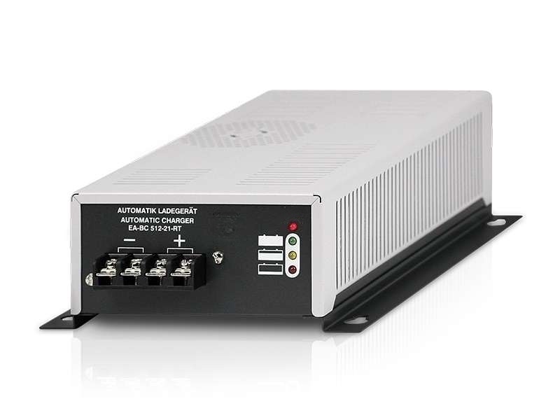
In the field of industrial automation, battery-powered systems have become increasingly important, especially for uninterrupted power supply in mission-critical applications. A European client specializing in compact, high-performance battery chargers for automation systems was seeking a reliable PCBA manufacturing partner to enhance product quality, reduce costs, and improve delivery timelines.
1. Background Overview A European industrial automation client required a compact, high-isolation, and cost-effective magnetic current sensor PCBA to be integrated into their control cabinet systems. The goal was to ensure safe and accurate current monitoring in a high-voltage industrial environment while maintaining stable performance under electromagnetic interference (EMI). 2. Application Scenario The current sensor […]
1. Background Overview A European customer specializing in voltage regulators was seeking to integrate a new high-performance voltage sensor module into their next-generation products. The client faced challenges such as unstable temperature drift, inefficient component layout, and long delivery cycles. They were looking for a reliable manufacturing partner with strong customization capabilities and ultimately chose […]
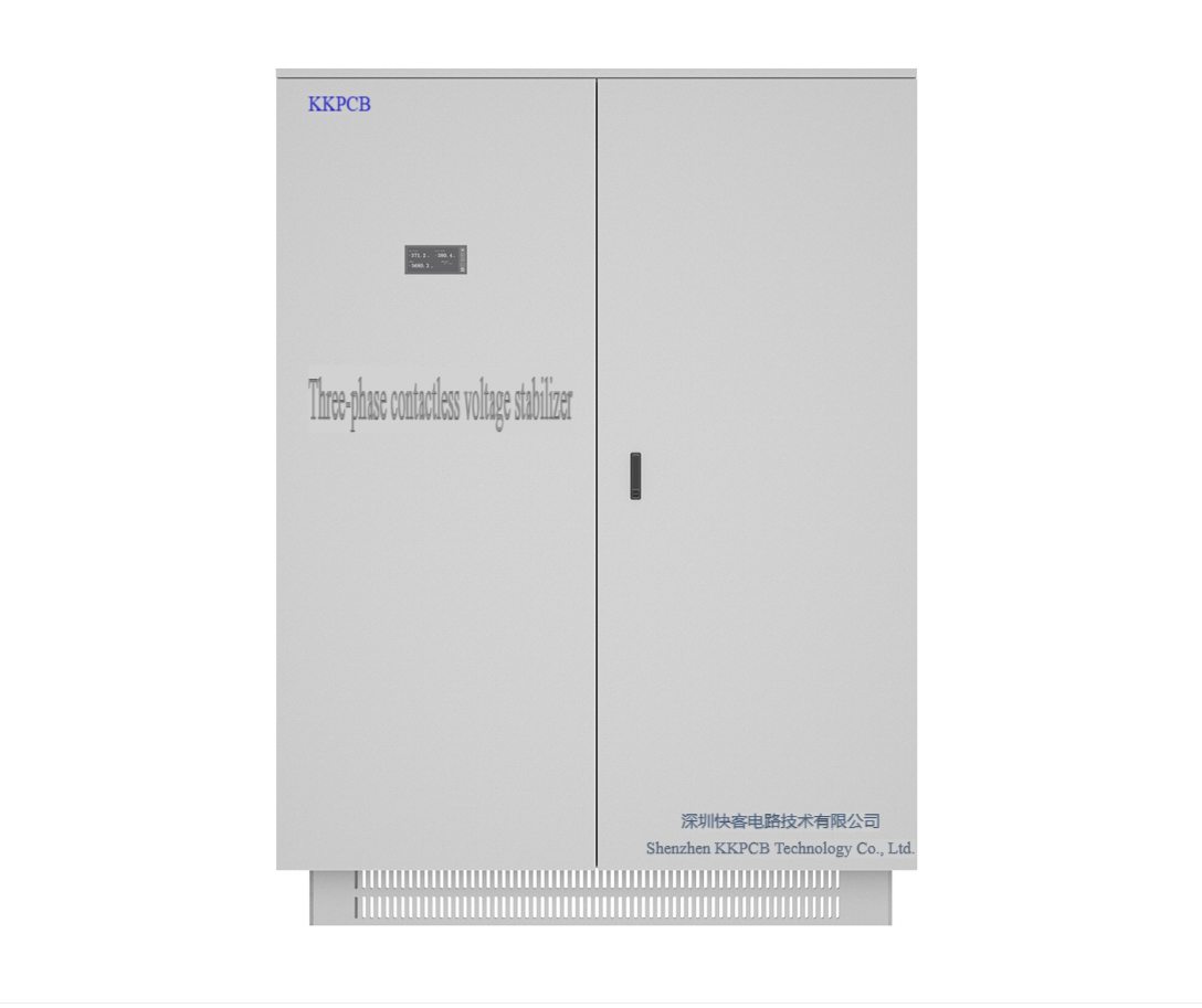
1. Background Overview In modern industrial automation systems, a stable and reliable power supply is critical for ensuring efficient equipment operation. A European client specializing in industrial-grade voltage regulators was seeking to enhance product performance in areas such as voltage stability, thermal control, communication reliability, and cost efficiency. They turned to KKPCB for a customized […]
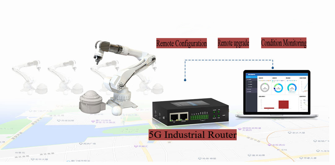
1. Background Overview A European customer in the industrial automation sector required a high-performance and reliable industrial network router for device-to-device communication in their automated systems. The router needed to support high-speed data transfer, strong anti-interference capabilities, remote control functionality, and stable operation in harsh environments. The customer was looking for a supplier with expertise […]
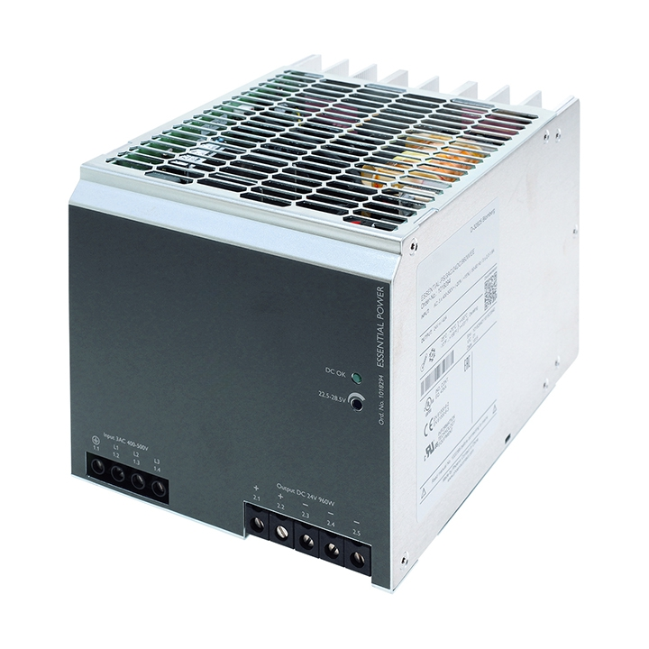
1. Background A European industrial automation customer was developing a power supply module for control systems, requiring high stability, conversion efficiency, and EMC compliance to ensure performance in demanding industrial environments. After evaluating several suppliers, the customer sought a reliable PCBA manufacturer with proven quality control and customization capabilities. 2. Application Scenario The power supply […]
1. Background Overview Under the accelerating global trend of industrial automation, a client from Europe aimed to develop a servo drive product with high dynamic response, high-precision control, and high integration for their next-generation industrial automation equipment. After evaluating multiple suppliers, the client ultimately chose to collaborate with KKPCB, seeking a one-stop customized service from […]
1️⃣ Background Overview With the tightening of global environmental regulations and the upgrading of industrial water resource management needs, sewage treatment plants of customers in Europe, America and the Middle East are in urgent need of highly reliable and extreme environment resistant automation control systems. Traditional PLC modules have pain points such as frequent signal […]


