


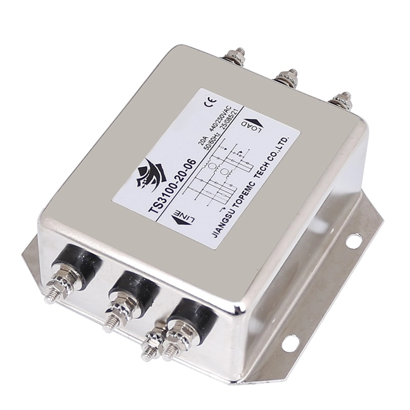
1. Background Overview A European client in the industrial automation sector was facing challenges related to electromagnetic interference (EMI) suppression, long lead times, and cost control in their power filter modules. They required a reliable manufacturing partner to deliver high-quality PCBA with strong EMI performance and timely delivery. KKPCB was selected for its advanced PCB […]
1. Background A European client in the industrial automation sector aimed to develop a compact, stable, and interference-resistant PLC programmer. Their previous supplier struggled with delivery delays and inconsistent quality, leading the client to seek a more reliable PCBA partner. KKPCB was selected for its strong manufacturing capabilities and engineering support. 2. Application Scenario The […]
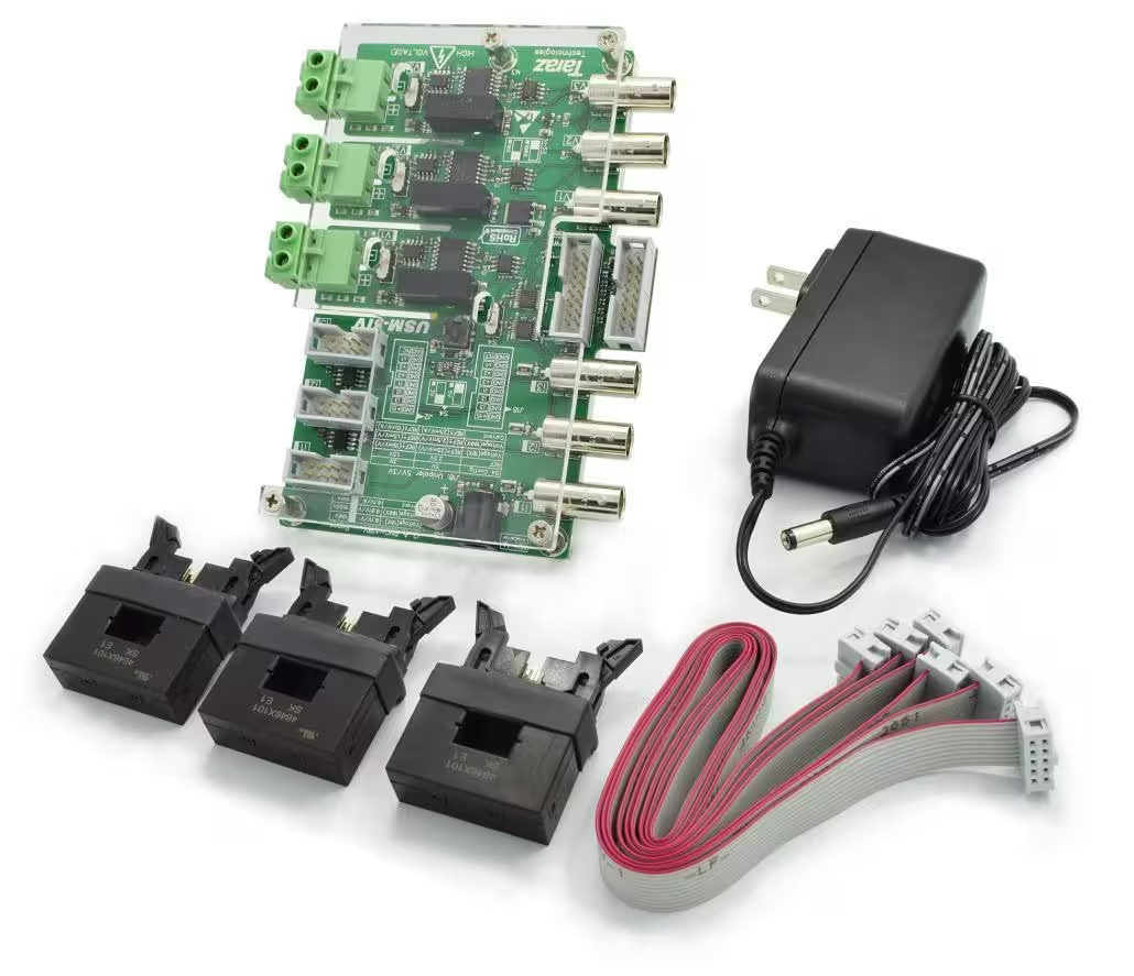
1. Background Overview A European client specializing in smart grid and power electronics required a high-precision, compact, and EMI-resistant voltage sensor module PCBA. The solution needed to support multi-channel voltage and current measurement, ensure signal isolation, and be compatible with various control systems. 2. Application Scenario The PCBA is integrated into power monitoring systems, including […]
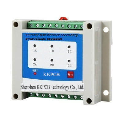
1. Background Overview A European industrial customer focusing on smart distribution systems required a highly accurate, low-loss, and production-friendly current transformer PCBA. The solution needed to integrate current sensing, energy monitoring, and protection features while maintaining cost-effectiveness and production scalability. 2. Application Scenario The PCBA is integrated into smart distribution cabinets, serving as the core […]
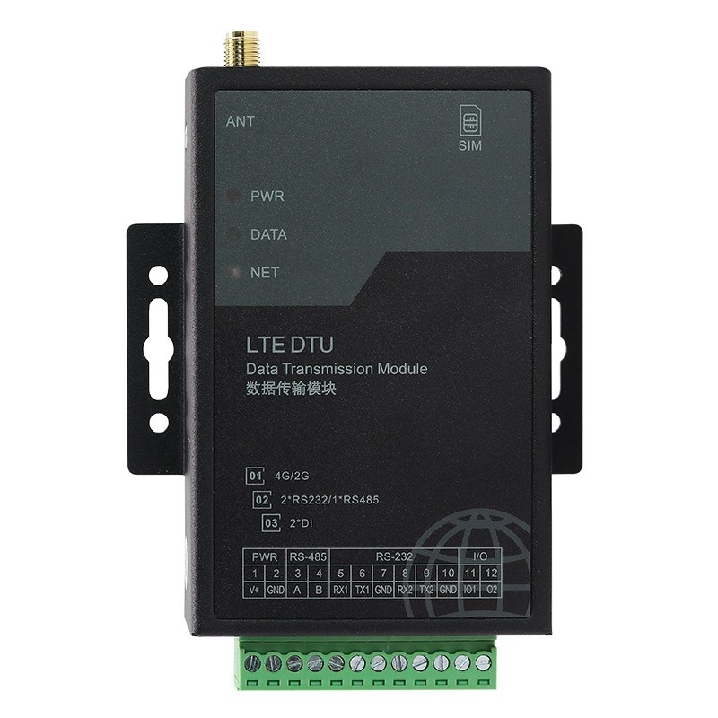
1. Background Overview A European industrial automation customer required a high-reliability data transmission module for use in rugged and space-constrained environments. The module needed to meet strict requirements for signal integrity, power efficiency, and heat dissipation, while ensuring fast production and stable long-term performance. 2. Application Scenario The PCBA is used in real-time data transmission […]
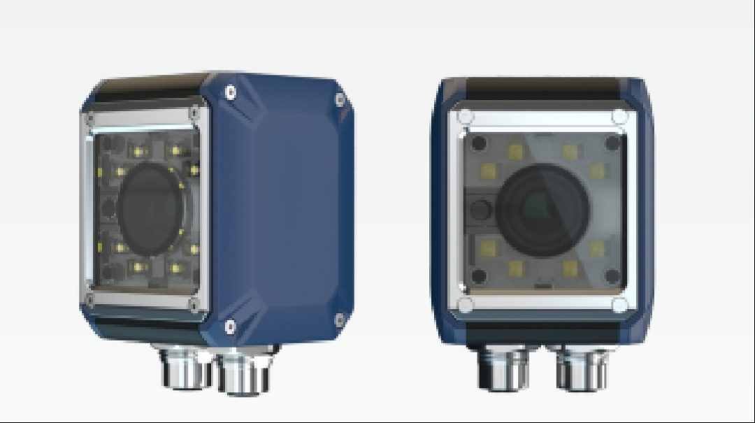
1. Background Overview A European client aimed to develop a high-performance industrial smart sensor for industrial automation systems. The device needed to be compact, highly reliable, and compatible with multiple sensor types, while supporting robust communication protocols and protection mechanisms. To meet their high reliability and mass production consistency requirements, the client partnered with KKPCB […]
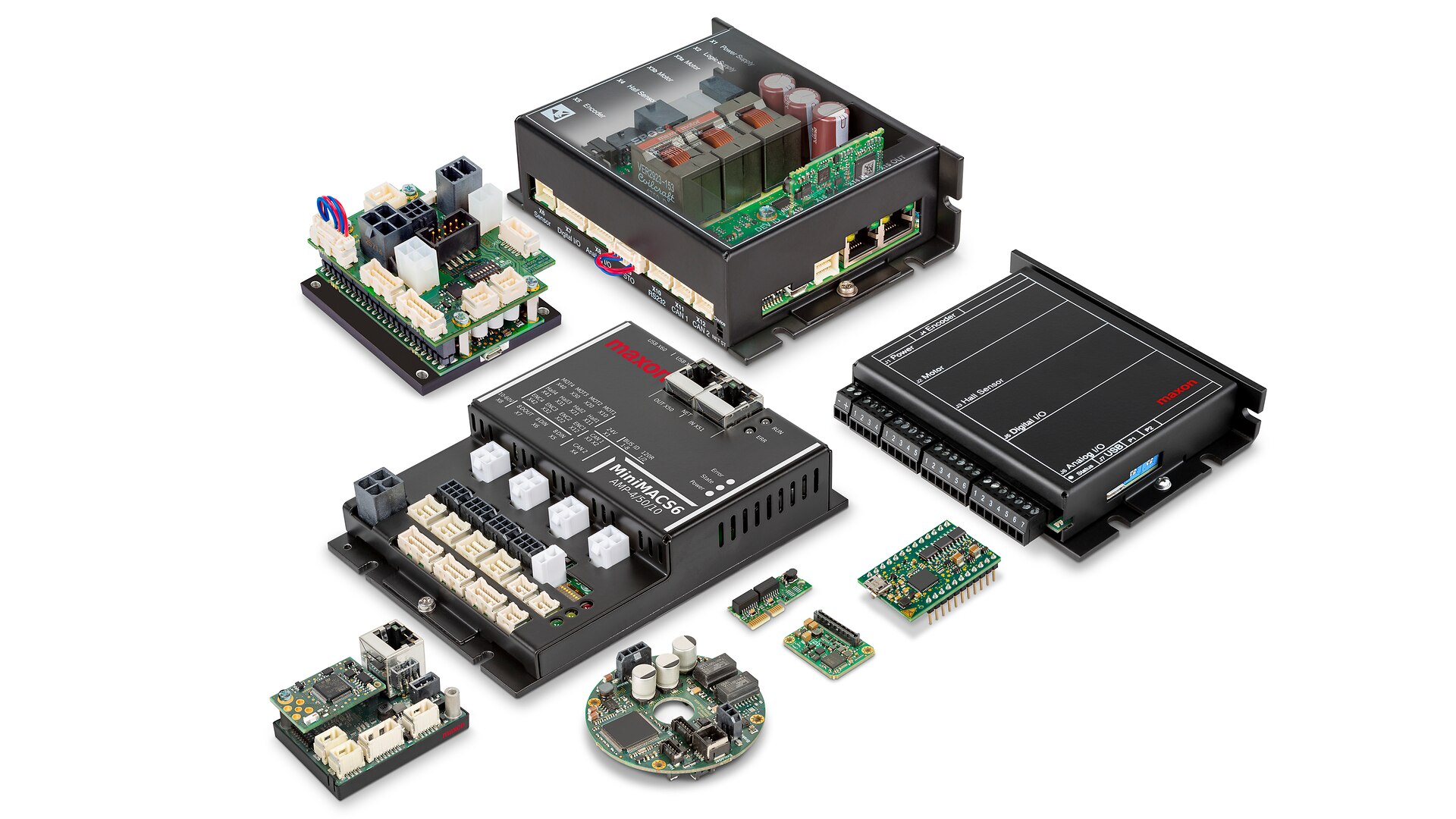
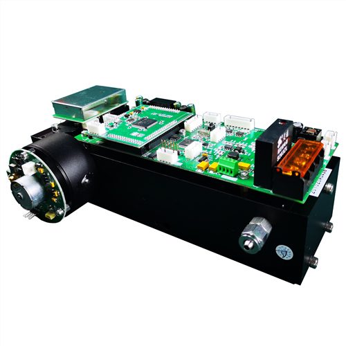
1. Background Overview A European customer sought to develop a compact, high-performance motor controller for use in industrial automation systems. The controller had to support precise motion control, offer robust communication interfaces, and maintain operational reliability in demanding environments. Due to the complexity of the design and need for high-quality production, the customer turned to […]
1. Background Overview With the rising demand for data processing and real-time analysis in industrial automation systems, high-speed and reliable data storage devices have become essential. A European industrial equipment manufacturer approached KKPCB for a customized PCBA solution for their new-generation data storage modules. The goal was to ensure high performance, reliability, and cost-efficiency under […]
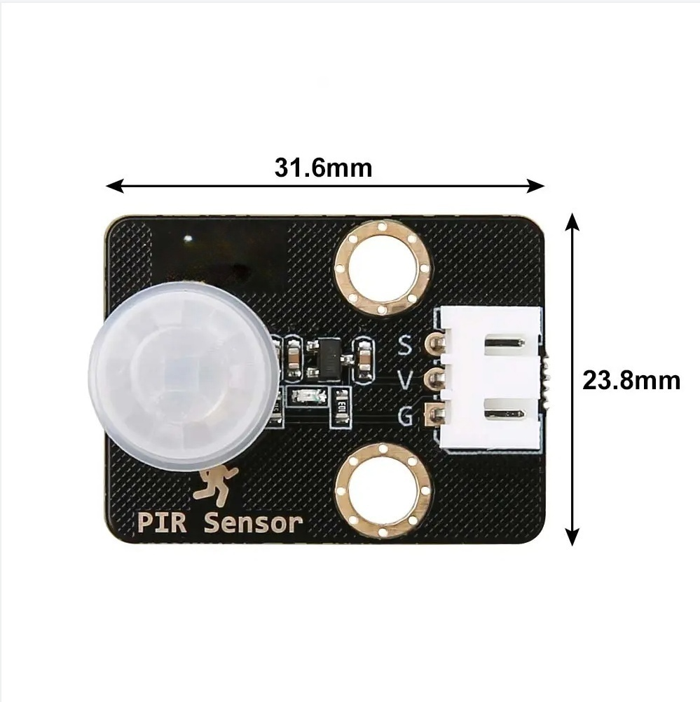
1. Background Overview In industrial automation systems, sensors play a vital role in enabling intelligent monitoring and equipment interaction. A European client recently sought to develop a PIR-based motion sensor module for use in equipment activity detection and control systems. The module required high sensitivity, strong anti-interference capability, low power consumption, and stable performance in […]
1. Background Overview With the growing demand for smart cities and industrial automation, air quality monitoring systems have become critical in factories, laboratories, smart buildings, and underground facilities. A European client developing a gas sensor module for air quality detection required a high-precision, low-power, and stable PCBA solution with strong anti-interference capability. KKPCB was selected […]