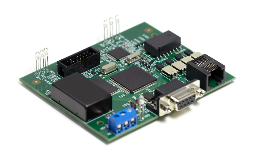
PCB solder mask is one of the important components in the PCB process. In-depth knowledge of solder mask will help engineers design PCBs with better functions and quality. This article will explore the composition of PCB solder mask and its important role.
Copper Core PCBs (CCPCBs) fall under the category of Metal Core PCBs, which use metal as a substrate, hence also known as Copper-Based PCBs. Similarly, Copper Core PCBs also use copper as a substrate, mainly because of the thermal conductivity properties of the material while maintaining the durability of the board itself
RF (Radio Frequency) PCB design is often described as a “black art” because there are still many uncertainties in theory, but this view is only partially correct. There are also many rules and regulations that can be followed in RF PCB design and should not be ignored
Addressing signal integrity (SI) issues early in the PCB design process can streamline the design and eliminate the need for corrective termination devices later. Here, we outline critical steps to maintain signal integrity, from planning through testing.
RF circuit board design is a critical and often complex area of PCB engineering. While there are many uncertainties in theory, practical design rules can be followed to optimize performance.
Key Takeaways
Defining two major concepts of board design and production: class and build.
An overview of the layout department’s responsibilities: library part generation as well as placement and routing.
Stepping more granularly through each task from schematic/design document reception to manufacturing files.


