


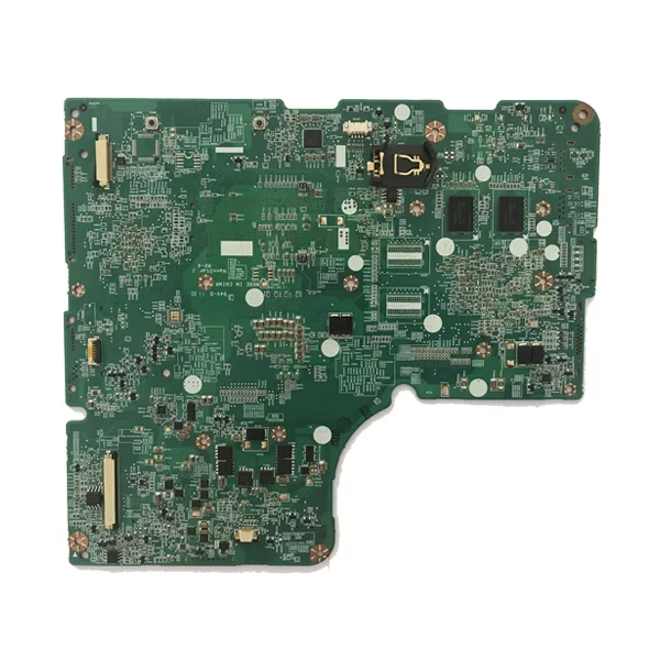
As the largest PCB manufacturer globally, China not only leads in production volume and technology but also continues to innovate. By increasing research and development investment and optimizing production processes, China’s PCB industry has gradually transitioned from low-end manufacturing to high-end production, especially excelling in areas such as high-frequency, high-speed, and high-precision applications. Meanwhile, China’s cost advantages, rich industrial chain resources, and mature supply chain management systems further solidify its dominant position in the global market.
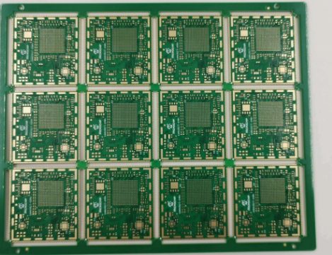
The manufacturing of HDI PCBs began in the late 1980s. With the successive production of PCBs, the first HDI production began in 1984. Since then, designers and manufacturers have been looking for ways to pack more components in a smaller area. HDI boards are designed and manufactured to comply with IPC-2315 and IPC-2226 standards.
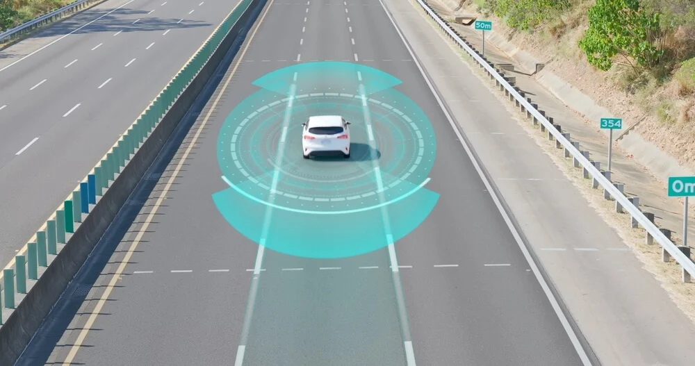
The Internet of Things (IoT) is revolutionizing industries worldwide, and its influence on Printed Circuit Board (PCB) design and manufacturing is profound. As IoT devices become more compact, efficient, and interconnected, the demand for innovative PCB designs has surged. This blog delves into how IoT is transforming PCB design and manufacturing, the challenges it poses, and the opportunities it presents.
Incorporating schematic simulation into the PCB design process not only saves valuable time but also increases the accuracy and efficiency of the entire workflow. By automating the process of checking for errors and verifying connections, designers can improve the overall quality of the PCB and minimize the chances of issues in the final design.
Inexperienced PCB designers often overlook critical checks in the later design stages, leading to issues like inadequate line width, misplaced silkscreens, and insufficient spacing near sockets. These errors can cause electrical or manufacturing issues, potentially requiring redesigns and increasing production costs. Below is a comprehensive list of essential PCB design checkpoints to ensure product quality and manufacturability.
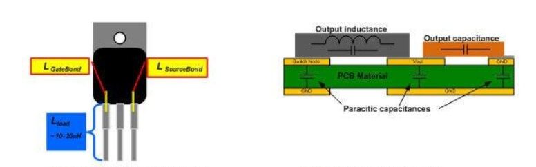
Based on recent trends, improving efficiency is a key goal, and the trade-off of using slow switching devices for better EMI is not worth it. Superjunctions can improve efficiency in applications where planar MOSFETs struggle. Superjunction MOSFETs significantly reduce on-resistance and parasitic capacitance compared to traditional planar MOSFET technology. The significant reduction in on-resistance and reduced parasitic capacitance, while helping to improve efficiency, also produces fast switching transitions of voltage (dv/dt) and current (di/dt), forming high-frequency noise and radiated EMI.
When discussing wiring-related technologies, two issues will be discussed: What if management cannot use a double-layer board or a ground plane, but still needs to reduce the noise in the circuit? And how to design the circuit to meet the ground plane requirements? Generally speaking, the solution is to tell management that a ground plane is necessary if reliable circuit performance is to be achieved. The main reason for using a ground plane is that the ground impedance is low and it can reduce EMI to a certain extent. But if cost constraints prevent users from achieving what they need, some suggestions provided in this article, such as star networks and correct current return paths, can also slightly reduce circuit noise.
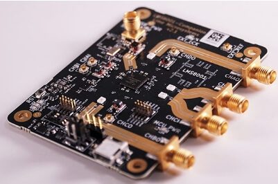
Microstrip patch antennas and their arrays may be rare but are the most widely used antenna form. They have a simple structure and can be formed by a dielectric, a metal conductor patch on the dielectric layer, and a ground plane. Even the dielectric in the middle can be an air structure. A typical microstrip patch antenna is made on a printed circuit board (PCB), and a fine line structure is etched on the conductive metal layer using a photocopying method
Whether the signal quality will be affected depends on the method of adding test points and how fast the signal is. Basically, the additional test points (without using the existing vias (via or DIP pins) as test points) may be added to the line or a short line may be pulled out from the line. The former is equivalent to adding a very small capacitor to the line, and the latter is an additional branch
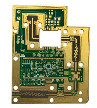
High-frequency circuit boards refer to special circuit boards with higher electromagnetic frequencies, and are one of the most difficult boards