


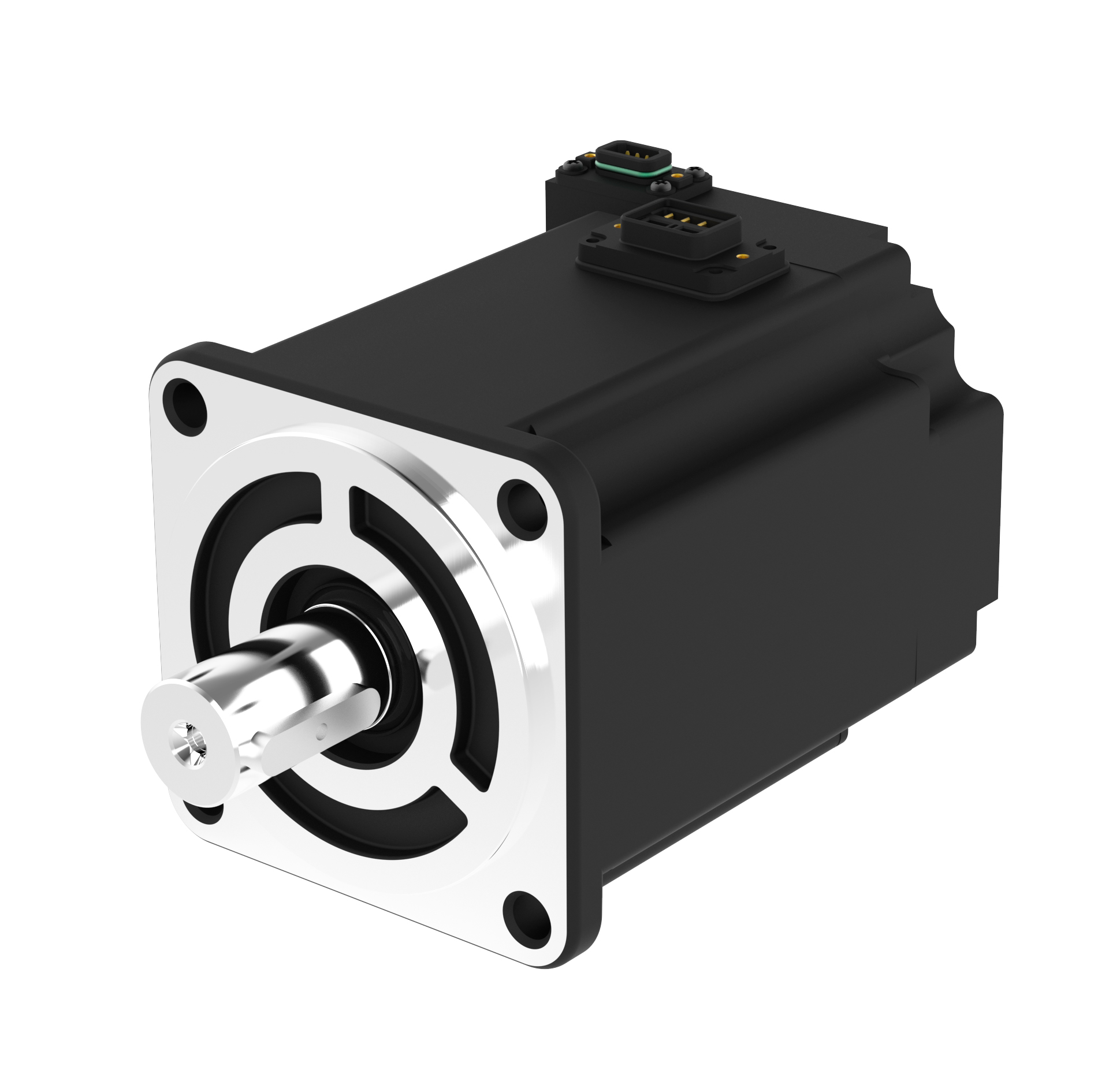
1. Background With the rapid evolution of industrial automation, AC servo motors have become critical components in motion control systems requiring precise speed and position control. One of our European customers developing a new generation of AC servo motors faced several challenges: unstable control performance, high EMI risks, complex assembly, and unpredictable lead times. They […]
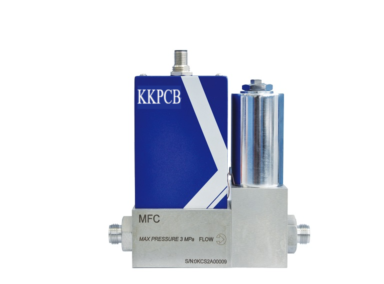
1. Background Overview A European client specializing in industrial automation sought a reliable and high-precision PCBA partner for their mass flow meter product. They needed a solution to improve measurement accuracy, ensure high durability under harsh industrial environments, and maintain competitive cost efficiency. 2. Application Scenario The mass flow meter is widely used in semiconductor […]
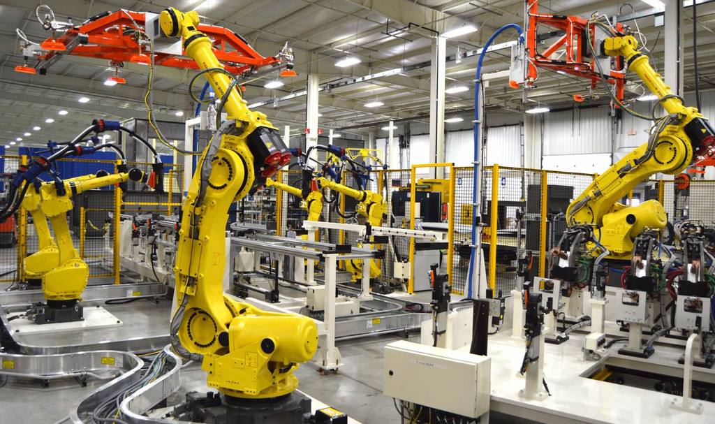
1. Background Overview With the growing adoption of industrial automation in Europe, an increasing number of companies are seeking compact, high-performance robot control systems to optimize production flexibility and operational efficiency. A European client approached us with a demand for a next-generation industrial robot control system PCBA, aiming for smaller size, faster processing speed, enhanced […]
1. Background Overview A European customer specializing in voltage regulators was seeking to integrate a new high-performance voltage sensor module into their next-generation products. The client faced challenges such as unstable temperature drift, inefficient component layout, and long delivery cycles. They were looking for a reliable manufacturing partner with strong customization capabilities and ultimately chose […]
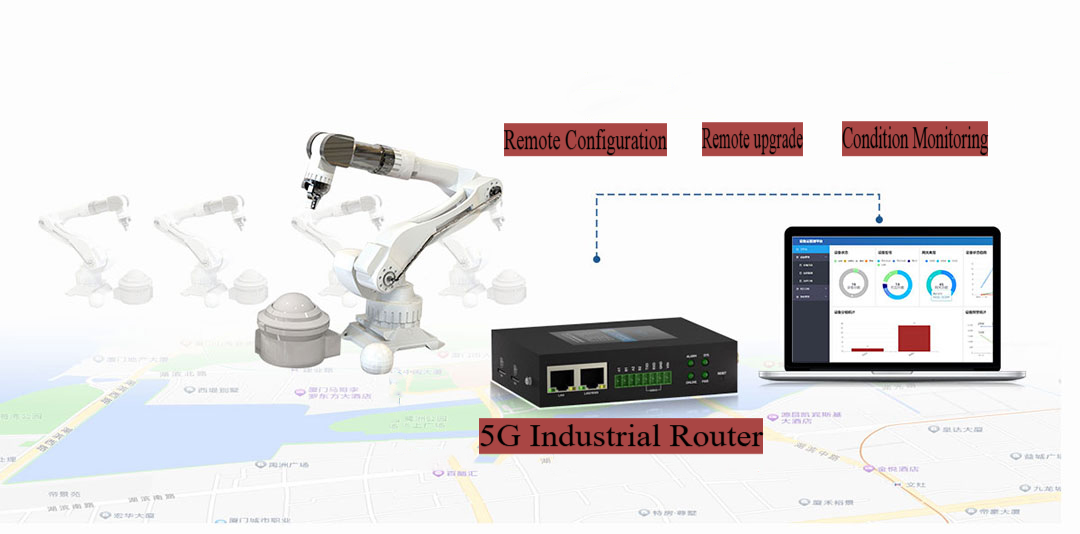
1. Background Overview A European customer in the industrial automation sector required a high-performance and reliable industrial network router for device-to-device communication in their automated systems. The router needed to support high-speed data transfer, strong anti-interference capabilities, remote control functionality, and stable operation in harsh environments. The customer was looking for a supplier with expertise […]
1. Background Overview Under the accelerating global trend of industrial automation, a client from Europe aimed to develop a servo drive product with high dynamic response, high-precision control, and high integration for their next-generation industrial automation equipment. After evaluating multiple suppliers, the client ultimately chose to collaborate with KKPCB, seeking a one-stop customized service from […]
1️⃣ Background Overview With the tightening of global environmental regulations and the upgrading of industrial water resource management needs, sewage treatment plants of customers in Europe, America and the Middle East are in urgent need of highly reliable and extreme environment resistant automation control systems. Traditional PLC modules have pain points such as frequent signal […]
There are three main sources of heat in PCB: heat from electronic components; heat from PCB itself; Heat from other parts.
Among the three heat sources, the heating from electronic components is the largest, followed by the heat generated by PCB board, and other heat from the outside based on the overall thermal design of the system.
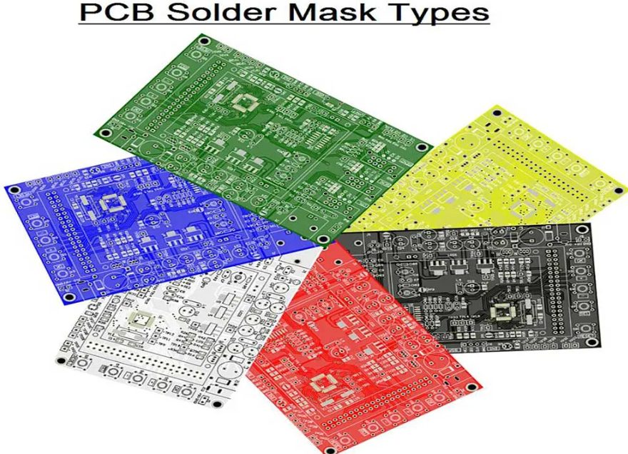
PCB solder mask is also known as PCB solder resist or PCB solder mask. It is a thin polymer protective layer PCB layer or coating that is applied on the copper traces to avoid initiating corrosion and oxidation processes after the PCB manufacturing process.
As electronic devices become more complex and ubiquitous, the need for reliable and high-performance PCBs continues to grow. PCB testing standards provide a framework for ensuring that these essential components meet industry benchmarks for safety, reliability, and functionality. Manufacturers who adhere to these testing standards are better positioned to deliver high-quality, dependable products, build trust with their customers, and minimize the risk of product failures. Whether through visual inspection, electrical testing, or advanced X-ray analysis, rigorous testing ensures that the PCBs will perform as expected, even in the most challenging environments.