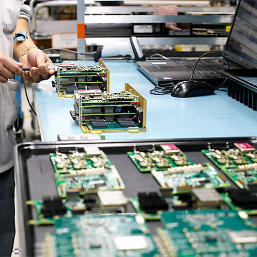
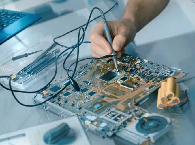
Troubleshooting printed circuit boards (PCBs) can be a daunting task, but with a systematic approach, it becomes manageable and efficient. This guide provides a step-by-step process to identify faulty components on PCBs, along with methods tailored to specific component types and advanced techniques for batch inspection.
Surface finishes in PCBs are vital for ensuring solderability, electrical conductivity, and corrosion resistance. They help components bond securely to the board, ensure smooth signal flow, and protect the PCB from environmental damage. Without a proper surface finish, a PCB may not function correctly or could wear out faster.
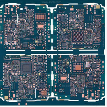
HDI Printed Circuit Board have a higher density of circuits per unit compared to traditional PCBs. Depending on the purpose, they are manufactured using various materials, such as FR4, metal, fiberglass, etc. In addition to microvias with a diameter of less than 0.006 inches, they also adopt buried vias and blind vias.
PCBs always face difficulties in designing. Many manufacturers have reported problems such as crosstalk, noise, and stray capacitance, which directly affect the performance level – whether it is a single-sided or double-sided PCB. This is when the concept of multi-layer PCB assembly
Designing a high-voltage PCB requires careful planning, adherence to specific guidelines, and a keen eye for safety. Whether you’re working on industrial equipment, power electronics, or consumer devices, the following tips and considerations will ensure you create efficient and safe high-voltage PCB designs.
A multilayer PCB is an advanced circuit board featuring multiple layers of conductive copper separated by insulating materials. This configuration is akin to a sandwich, where the copper layers serve as the bread, and the insulating material acts as the filling.
Multilayer PCBs (Printed Circuit Boards) are integral to modern electronics, offering unparalleled performance in compact designs. While they come with several benefits, they also present unique challenges.
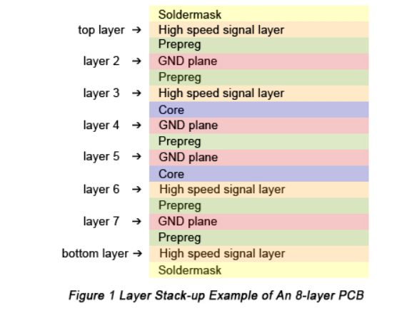
Stack-up refers to the arrangement of copper layers and insulating layers that make up a PCB prior to board layout design. While a layer stack-up allows you to get more circuitry on a single board through the various PCB board layers
Printed circuit boards (PCBs) are the core of most electronics today, determining basic functions through combinations of components and wiring mechanisms. Most PCBs of the past were relatively simple and limited by manufacturing techniques, while today’s PCBs are much more complex. From advanced flexible options to odd-shaped varieties, PCBs are much more varied in nowadays’ world of electronics
When designing high-speed PCBs, understanding the core concepts is crucial for ensuring efficiency and functionality. This guide introduces key elements such as layers, vias, pads, and more to help beginners and professionals alike.
- 1
- 2

