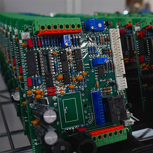
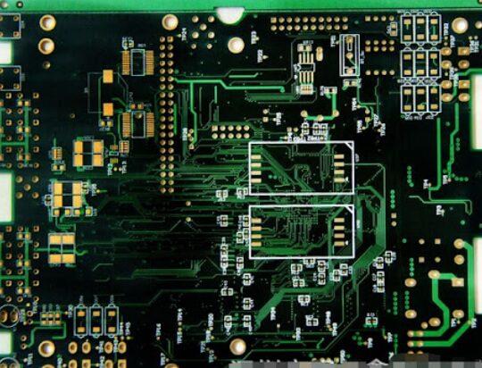
Generally, multilayer circuit boards are designed with large amounts of copper foil as grounding devices. Sometimes, the Vcc layer is also designed with large amounts of copper foil. When these large amounts of copper foil cannot be evenly distributed on the same multilayer circuit board, it will cause problems with uneven heat absorption and heat dissipation rates. The multilayer circuit board will naturally expand and contract when heated and contract when cooled. If the expansion and contraction cannot be achieved at the same time, different ground stresses will be caused and the board will deform. At this time, if the temperature of the board has reached the limit of the Tg value, the board will gradually soften and cause deformation
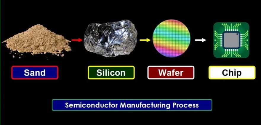
In order for silicon to turn into a semiconductor chip, it needs to go through the several complex process of wafer manufacturing, oxidation, photolithography, etching, deposition and ion implementation, metal wiring, Eds and packaging.
This article starts with the most basic PCB layout and discusses the role and design techniques of PCB layer stacking in controlling EMI radiation
- 1
- 2

