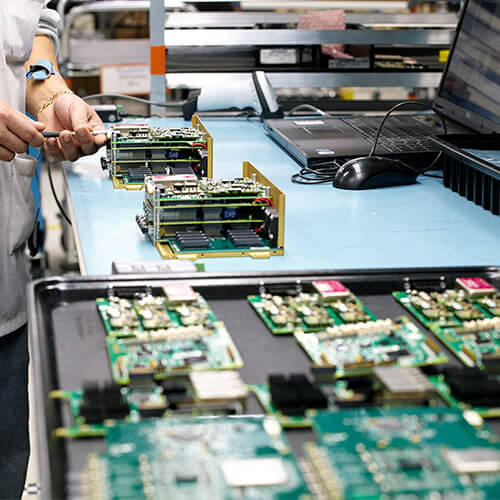
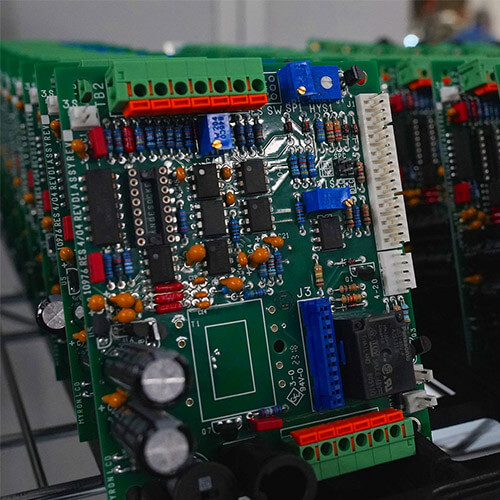
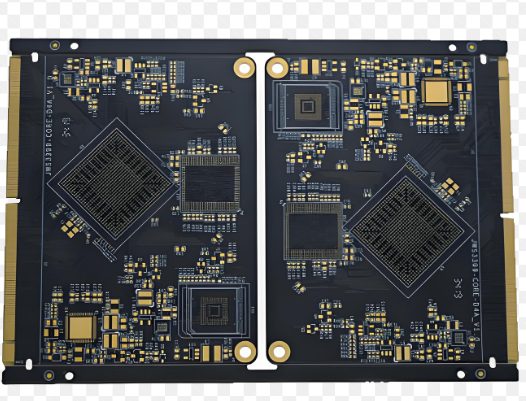
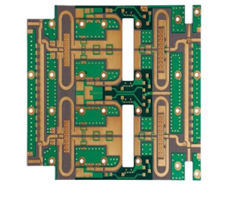
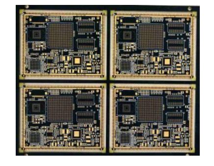
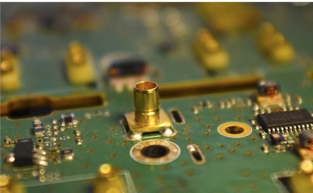
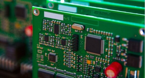
A Multilayer PCB (Printed Circuit Board) is a type of PCB with more than two conductive layers. Unlike a double-sided PCB, which has two copper layers (top and bottom), a multilayer PCB consists of three or more layers of copper, interconnected by copper-plated vias. The number of layers can range from 3 layers to 40 layers or more, depending on the design requirements
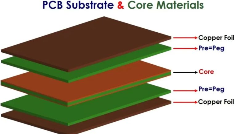
The Printed Circuit Board (PCB) is a fundamental component in all modern electronics, providing the platform for the electronic components and circuits. The performance, durability, and overall quality of a PCB are heavily influenced by the materials used for its substrate and core. This comprehensive guide explores the different types of PCB substrate and core materials, their properties, applications, and why they are important for engineers, PCB manufacturers, and students.
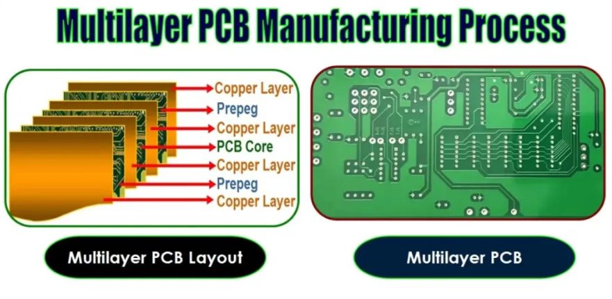
A multilayer PCB is a printed circuit board that consists of more than two layers, typically at least three or more layers of conductive copper, separated by an insulating material (substrate). These layers are stacked and connected by vias, resulting in a compact and efficient PCB design.
The nearly isotropic dielectric constant (ϵr\epsilon_rϵr) of RT-duroid® 5870 – 5880 laminates, attributed to their glass microfiber-reinforced PTFE composition, offers several key benefits for high-frequency applications.
A printed circuit board, commonly known as a PCB, is an assembly that uses copper conductors and electricity to create electrical connections between electrical components. PCB manufacturers use a substrate to make it, which houses the components that form the basis of the PCB. PCBs are made of a variety of substrate materials, depending on the requirements of the circuit.
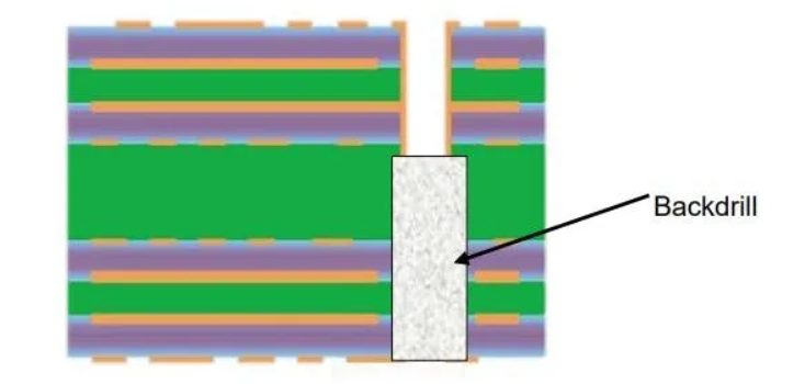
Back drilling is a method to remove the via stub from the specific layer of multilayer PCB. Via stub is a non-functional portion of a plated through hole or via barrel which can cause unwanted reflection leading to signal distortion and lower performance. It is recommended that the diameter of the back drill hole be greater than that of the via hole size.
By applying the guidelines in this article around stackup sequence, material selection, hole registration, panelization and thermal management, engineers can fully utilize 10 or more layers for their complex designs. Partnering with a shop experienced in high layer count boards ensures achieving the quality and functionality required to maximize your product’s capabilities and service life.
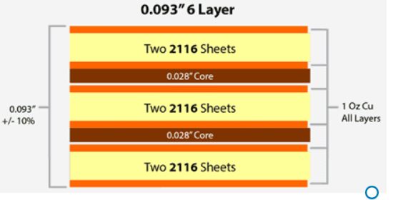
Printed circuit boards (PCBs) have evolved from simple single or double layer boards to complex multilayer boards with 6 or more layers to accommodate increasing component density and interconnectivity needs. 6 layer PCBs provide more flexibility for routing, plane separation and enable partitioning of circuits across layers.
A multilayer PCB, or Printed Circuit Board, is an advanced type of circuitry that facilitates complex electronic functionalities within a compact framework.
PCB layering or stacking is a way of stacking multiple printed circuit boards together while ensuring that there are predefined interconnections between them, allowing multiple printed circuit boards to be installed in the same device. These multi-layer PCBs can multiply the speed and functionality of a device and are composed of at least three conductive layers, with the bottom layer being composited with an insulating board
- 1
- 2

