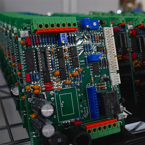
Printed Circuit Boards (PCBs) are a fundamental component in electrical engineering. They are used to create electronic circuits by arranging components such as transistors and resistors on a copper-based wiring pattern on the surface of an insulator (typically plastic) and then soldering them.
RT-duroid® 6002 laminates are widely used in high-frequency and microwave applications due to their excellent electrical and mechanical properties. Drilling is a critical step in fabricating bonded assemblies and multilayer boards with RT-duroid materials. Following the proper guidelines ensures clean vias, prevents delamination, and maintains structural integrity.
When applied correctly, copper coating offers more benefits than drawbacks, providing improved performance, noise reduction, and thermal management for PCBs. However, to achieve the best results, it’s crucial to carefully consider the design, including grounding, copper areas, and the specific requirements of high-frequency or low-frequency circuits. By paying attention to these details, designers can optimize the copper coating for better overall performance.
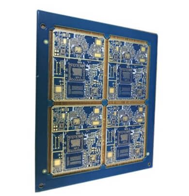
Multilayer PCB design follows principles similar to double-layer design, with added structural complexity and a focus on stable signal integrity and efficient routing. With experience in double-layer PCBs, moving to multilayer designs can be manageable.
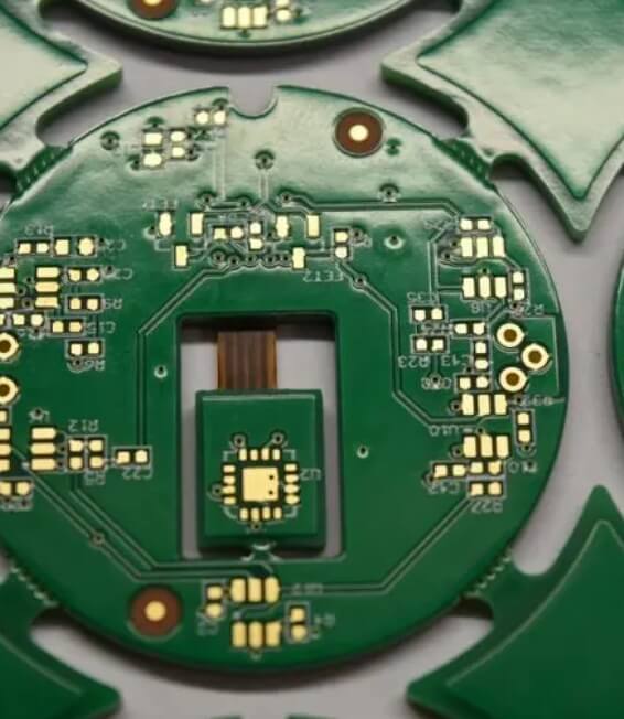
These PCBs create a more challenging design for rigid-flex manufacturers, but we’ve been able to supply successful designs with full compliance and reliability. By engineering these in a 3D environment, we’re able to achieve spatial efficiency and incorporate folds and flexes to help you meet the desired shape that works best with your application.
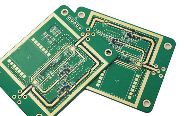
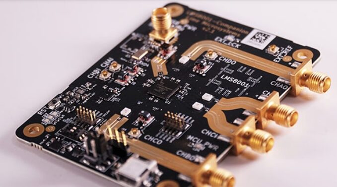
With the rapid development of electronic technology and the widespread application of wireless communication technology in various fields, high frequency, high speed and high density have gradually become one of the significant development trends of modern electronic products. The high frequency and high speed digitalization of signal transmission force PCB to move towards micro-holes and buried/blind holes, fine wires, and uniform thin dielectric layers. High-frequency, high-speed, high-density multi-layer PCB design technology has become an important research field. This time, we mainly want to learn some practical skills in high-frequency PCB design.

