


Client: A Leading Metro System Operator (Asia)Application: Underground Tunnel Communication Systems 1. Operational Challenges Environmental Conditions: Critical Failures Observed:▶ Insulation resistance (IR) dropped to <1GΩ within 6 months▶ Bit Error Rate (BER) surged to 10⁻⁴ (vs. required 10⁻⁸)▶ Frequent corrosion-induced signal loss (3+ annual maintenance interventions) 2. KKPCB’s Robust Manufacturing Solution Core Technical Innovations Technology […]
Client Industry: European Industrial Equipment ManufacturerApplications: Particle Accelerator RF Systems / Industrial Microwave Heating 1. Industry Manufacturing ChallengesCritical Requirements: Previous Supplier Issues:▶ CTE mismatch in traditional aluminum substrates caused copper layer delamination▶ Manual MOSFET soldering led to ±15% thermal resistance variation▶ Water-cooling solutions increased system complexity by 30% 2. Advanced Manufacturing Solutions (A) Core Process […]
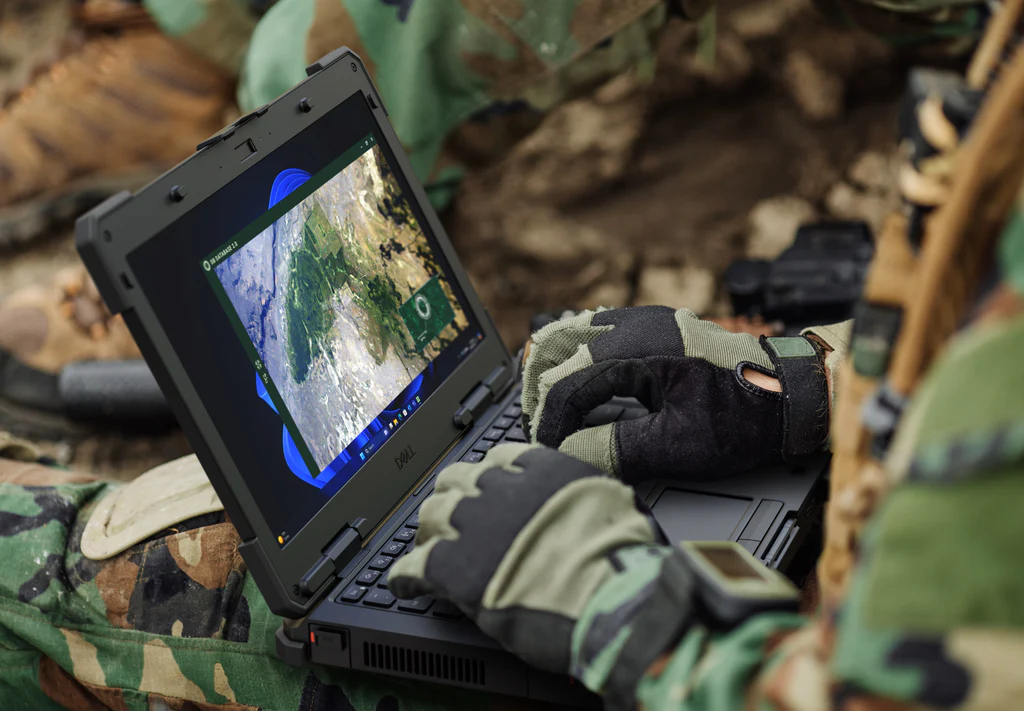
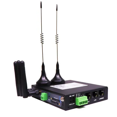
Industry: Defense Electronics
End Applications:
Armored vehicle main control units
Field communication relay equipment
Manufacturing Challenges:
Heterogeneous material processing (AlSiC metal substrate + FR4 multilayer hybrid lamination)
Extreme environment reliability (MIL-STD-810H vibration compliance)
Military-grade quality control (100% inspection + batch traceability)
Previous Supplier Pain Points:
✔ AlSiC substrate yield only 65% (delamination due to CTE mismatch)
✔ PCIe gold finger contact failure rate 3,000 PPM (post-vibration)
✔ EMP shielding layer vacuum lamination yield below 80%
1. Project Background
Industry: Satellite Communications/Military Radar
Application Scenario:
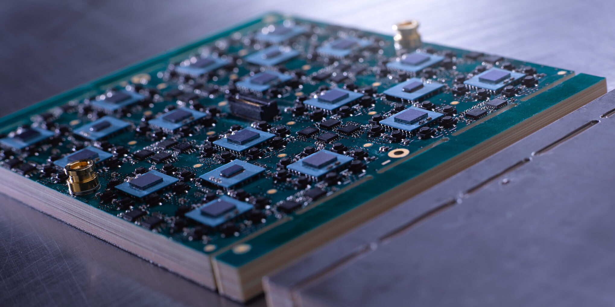
256-channel phased array antenna system (28GHz Ka-band)
Customer requirements: ±60° beam steering, ±0.5dB amplitude consistency, 8-week delivery
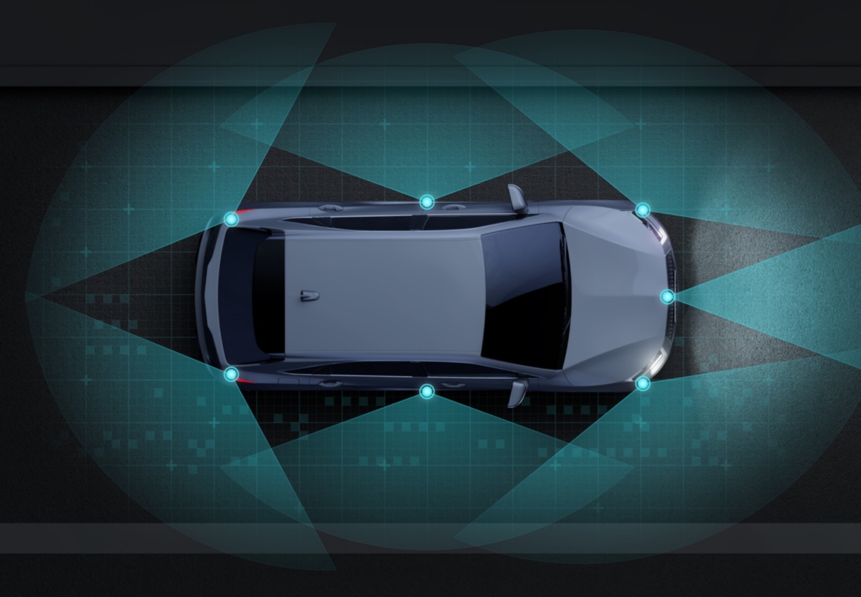
1. Customer Profile Client: AnonymousIndustry: ADAS (Advanced Driver Assistance Systems), Autonomous VehiclesApplication: 77GHz Long-Range Radar (LRR) for Highway Pilot & Collision Avoidance Customer’s Requirements: Key Challenges: 2. KKPCB’s Radar PCBA Solution (A) Material & Stackup Layer Material Function Key Specs RF Layers Rogers RO3003 Antenna Array & Front-End Dk=3.0, Df=0.0013 @ 77GHz Core Arlon 25FR […]

The customer is a globally leading manufacturer of communication equipment, specializing in the development and production of large-scale routers, switches, servers, and high-speed networking devices. As modern network communications demand increasingly high signal integrity, reliability, and thermal stability, the customer required an 18-layer PCB with low-loss material (S1000-2M) and advanced immersion gold plating to ensure stable signal transmission and long-term reliability
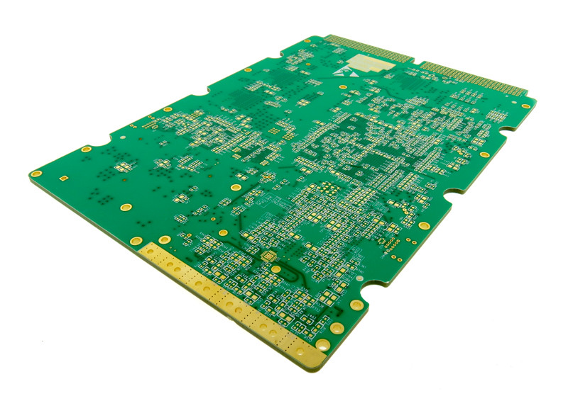
Advanced PCBs are complex multi-layer printed circuit boards (PCBs) with significantly more layers than standard multi-layer boards. These advanced PCBs are crucial for high-end, high-precision electronic devices, which are typically found in industries like industrial equipment, instrumentation, automotive electronics, aviation, military applications, communication systems, complex computing, and space technology.
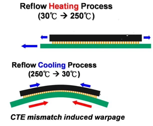
When designing and manufacturing Printed Circuit Boards (PCBs), one common yet often overlooked issue is warpage. Warping occurs when the PCB bends or twists, leading to alignment issues during assembly. This deformation can cause misalignment of components, poor solder joints, and even failure of the final product.
In modern electronic devices, the performance of control boards directly impacts the reliability and accuracy of the entire system. Whether in industrial automation, medical devices, or consumer electronics, data acquisition and signal processing boards (DAQ and Signal Processing PCBs) play a crucial role. To ensure that the system can efficiently and accurately process signals from sensors and other electronic components, optimizing PCB design is essential.
We explore how to optimize data acquisition and signal processing capabilities for control boards in high-precision PCB manufacturing and provide practical tips to help you achieve high-performance electronic systems.
The client specializes in the development and production of a wide range of microwave electronic products. These products are extensively used in satellite communication, television broadcasting, long-range communication, data and image transmission, radar, remote control, remote sensing, electronic reconnaissance, and electronic countermeasures. With deep technical expertise in microwave technology and high-frequency electronic products, the customer serves multiple high-tech industries requiring precise, reliable, and high-frequency transmission solutions.