“Enabling Next-Gen LEO Satellite Communication with High-Performance RF PCBs” Project Overview Customer Background A leading European satellite technology provider (identity protected under NDA) required high-reliability PCBs for their next-generation low Earth orbit (LEO) communication terminals, targeting IoT and global broadband connectivity. The system demanded ultra-low-loss signal transmission at Ka-band (26.5-40GHz) to meet ITU-R S.465-6 radiation […]
1. Customer Challenge
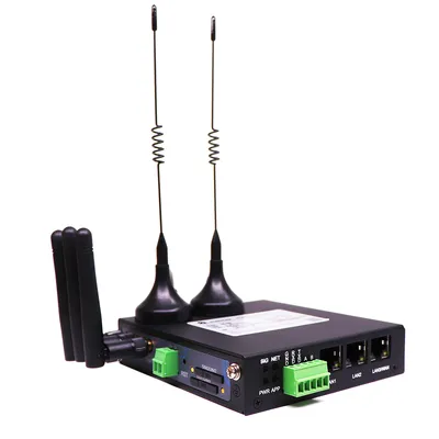
Application: Military/5G Base Station SDR Backplane
Critical Requirements:
Support 12 independent RF channels without interference
Achieve cross-channel isolation >65dB @2.4GHz
Pass FCC Part 90 certification for industrial radio equipment
Withstand harsh environments (85°C/85%RH for 1,000+ hours)
1. Customer Requirements
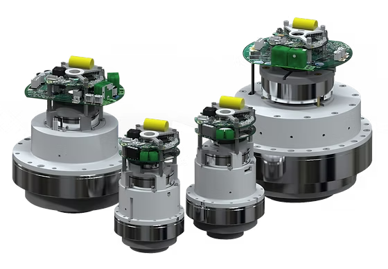
Application: Industrial robotic joint drive control
Key Challenges:
Integrate 16-channel PWM control + current sampling within 80mm × 60mm
Excessive MOSFET temperature rise (>30°C @20A), causing throttling
Compliance with IEC 61000-6-4 (Industrial EMC Standard)
Client: A Leading Metro System Operator (Asia)Application: Underground Tunnel Communication Systems 1. Operational Challenges Environmental Conditions: Critical Failures Observed:▶ Insulation resistance (IR) dropped to <1GΩ within 6 months▶ Bit Error Rate (BER) surged to 10⁻⁴ (vs. required 10⁻⁸)▶ Frequent corrosion-induced signal loss (3+ annual maintenance interventions) 2. KKPCB’s Robust Manufacturing Solution Core Technical Innovations Technology […]
Client Industry: European Industrial Equipment ManufacturerApplications: Particle Accelerator RF Systems / Industrial Microwave Heating 1. Industry Manufacturing ChallengesCritical Requirements: Previous Supplier Issues:▶ CTE mismatch in traditional aluminum substrates caused copper layer delamination▶ Manual MOSFET soldering led to ±15% thermal resistance variation▶ Water-cooling solutions increased system complexity by 30% 2. Advanced Manufacturing Solutions (A) Core Process […]
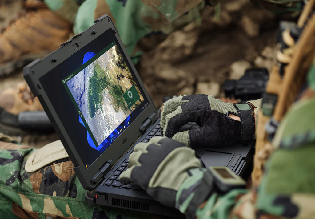
Industry: Defense Electronics
End Applications:
Armored vehicle main control units
Field communication relay equipment
Manufacturing Challenges:
Heterogeneous material processing (AlSiC metal substrate + FR4 multilayer hybrid lamination)
Extreme environment reliability (MIL-STD-810H vibration compliance)
Military-grade quality control (100% inspection + batch traceability)
Previous Supplier Pain Points:
✔ AlSiC substrate yield only 65% (delamination due to CTE mismatch)
✔ PCIe gold finger contact failure rate 3,000 PPM (post-vibration)
✔ EMP shielding layer vacuum lamination yield below 80%
1. Project Background
Industry: Satellite Communications/Military Radar
Application Scenario:
256-channel phased array antenna system (28GHz Ka-band)
Customer requirements: ±60° beam steering, ±0.5dB amplitude consistency, 8-week delivery
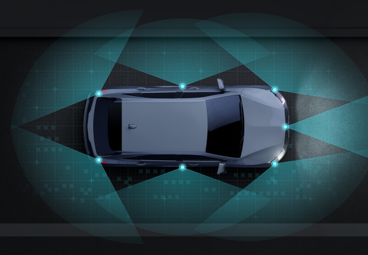
1. Customer Profile Client: AnonymousIndustry: ADAS (Advanced Driver Assistance Systems), Autonomous VehiclesApplication: 77GHz Long-Range Radar (LRR) for Highway Pilot & Collision Avoidance Customer’s Requirements: Key Challenges: 2. KKPCB’s Radar PCBA Solution (A) Material & Stackup Layer Material Function Key Specs RF Layers Rogers RO3003 Antenna Array & Front-End Dk=3.0, Df=0.0013 @ 77GHz Core Arlon 25FR […]
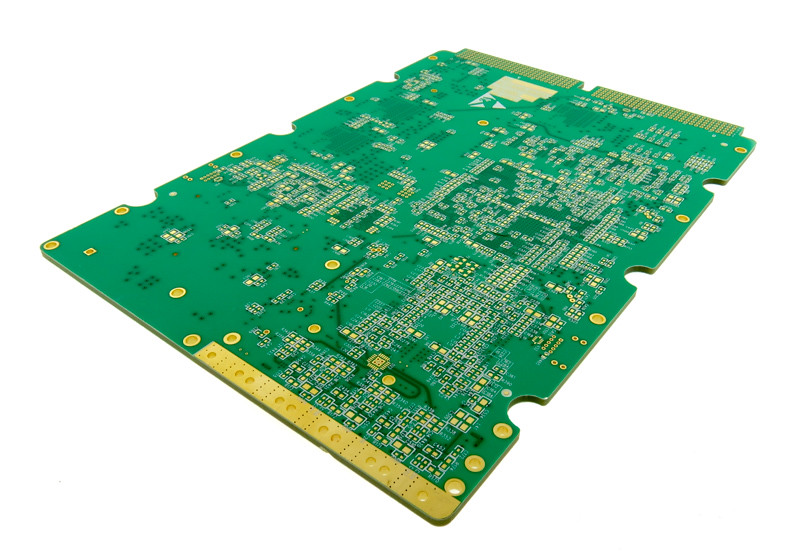
The customer is a globally leading manufacturer of communication equipment, specializing in the development and production of large-scale routers, switches, servers, and high-speed networking devices. As modern network communications demand increasingly high signal integrity, reliability, and thermal stability, the customer required an 18-layer PCB with low-loss material (S1000-2M) and advanced immersion gold plating to ensure stable signal transmission and long-term reliability
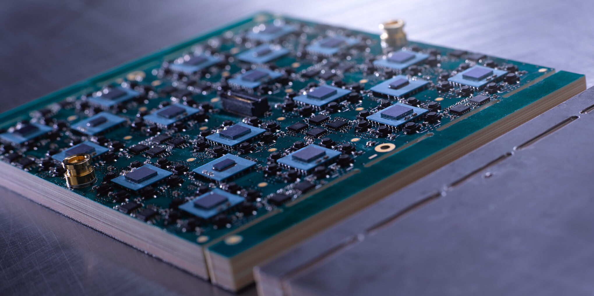
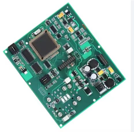
Advanced PCBs are complex multi-layer printed circuit boards (PCBs) with significantly more layers than standard multi-layer boards. These advanced PCBs are crucial for high-end, high-precision electronic devices, which are typically found in industries like industrial equipment, instrumentation, automotive electronics, aviation, military applications, communication systems, complex computing, and space technology.

