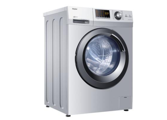
With the rapid development of the Internet of Things (IoT) and smart homes, smart home appliances have gradually become an important part of modern families. With its rich experience in the field of smart hardware and software integration, KKPCB has developed a smart washing machine APP for home appliance manufacturers, aiming to enhance the user’s laundry experience, realize remote control, smart reminders and equipment management, and make the laundry process more convenient and efficient.
I. Strategic Market Positioning
Industry Pain Points
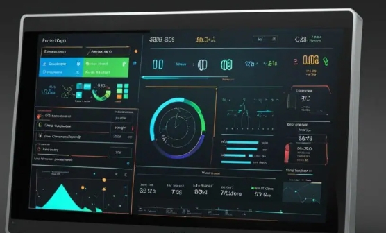
Limitations of Traditional Interfaces: 62% of Industrial Operators Express Frustration with Outdated HMI Systems (ABI Research 2024)
Multi-Platform Integration: Growing Demand for Unified Control across IoT/Operational Technology (OT) Systems
Safety Compliance: EN 61000-6-2/-4 Standards Become Mandatory for Industrial HMI
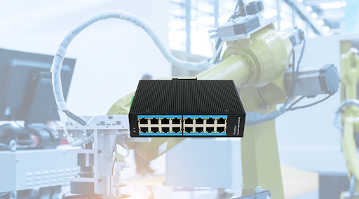
1. Background As industrial automation continues to evolve, a European client sought to develop a rugged, high-performance industrial Ethernet switch capable of operating in harsh environments with excellent anti-interference capability. The client required a reliable PCBA partner to meet strict demands in product quality, electromagnetic compatibility (EMC), and delivery schedule. KKPCB was selected as the […]
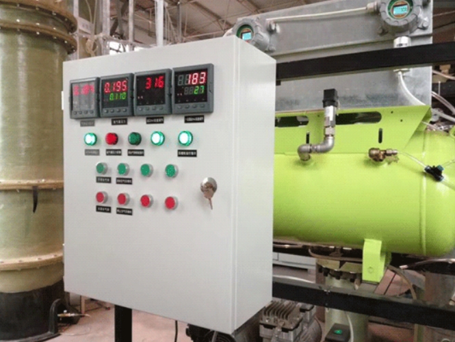
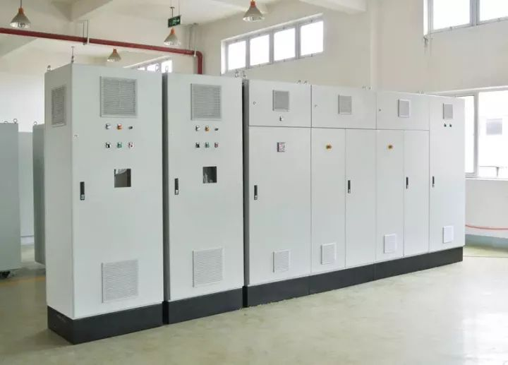
NHR-5400 Series 60-segment AI Temperature Controller was used to upgrade the temperature control system of the single crystal furnace, replacing the imported temperature controller.
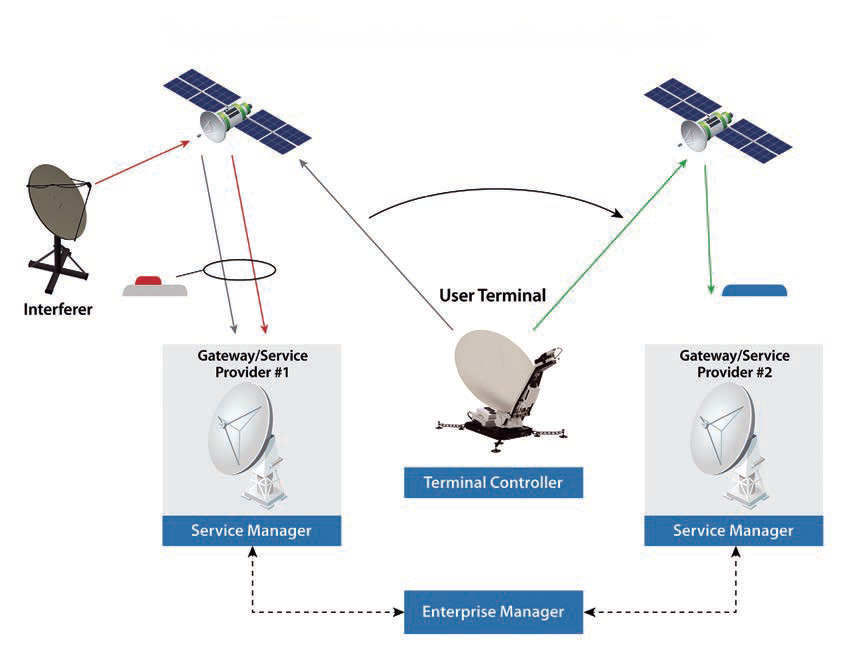
Client: A Leading Global Satellite Communications Provider (Confidential)
Application: Geostationary (GEO) Ka-band User Terminal (32×32 MIMO Array)
1. Background Overview A European customer specializing in voltage regulators was seeking to integrate a new high-performance voltage sensor module into their next-generation products. The client faced challenges such as unstable temperature drift, inefficient component layout, and long delivery cycles. They were looking for a reliable manufacturing partner with strong customization capabilities and ultimately chose […]
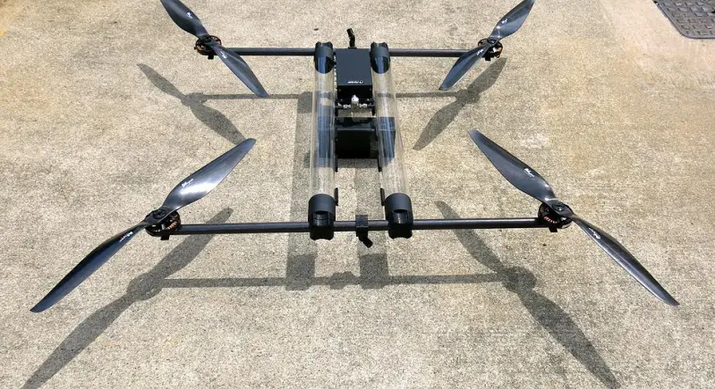
“Reducing Weight by 40% While Maintaining Robustness for Harsh Environment Operations” Project Overview Customer Background A European UAV manufacturer specializing in industrial surveillance (identity protected) required a weight-optimized RF PCBA for their next-generation drone’s communication module, targeting multi-band operation (900MHz/2.4GHz/5.8GHz). The legacy design’s excessive weight (120g) limited flight time, while inadequate environmental protection caused failures […]
“Enabling Next-Gen LEO Satellite Communication with High-Performance RF PCBs” Project Overview Customer Background A leading European satellite technology provider (identity protected under NDA) required high-reliability PCBs for their next-generation low Earth orbit (LEO) communication terminals, targeting IoT and global broadband connectivity. The system demanded ultra-low-loss signal transmission at Ka-band (26.5-40GHz) to meet ITU-R S.465-6 radiation […]
1. Customer Challenge
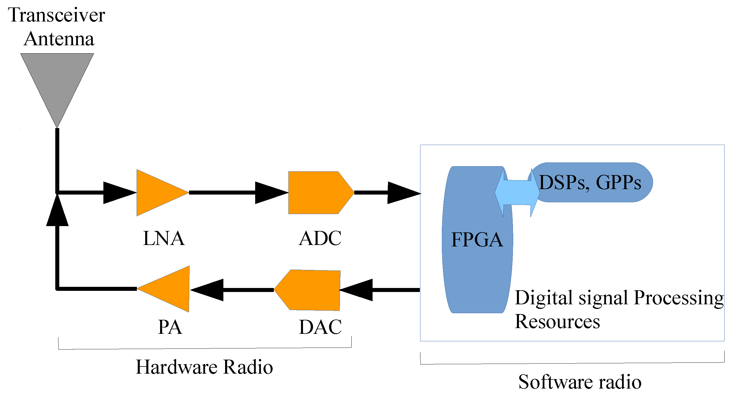
Application: Military/5G Base Station SDR Backplane
Critical Requirements:
Support 12 independent RF channels without interference
Achieve cross-channel isolation >65dB @2.4GHz
Pass FCC Part 90 certification for industrial radio equipment
Withstand harsh environments (85°C/85%RH for 1,000+ hours)
1. Customer Requirements
Application: Industrial robotic joint drive control
Key Challenges:
Integrate 16-channel PWM control + current sampling within 80mm × 60mm
Excessive MOSFET temperature rise (>30°C @20A), causing throttling
Compliance with IEC 61000-6-4 (Industrial EMC Standard)

