Electronic devices have transformed modern life, and at the heart of these innovations lies a critical component: the Printed Circuit Board (PCB). From smartphones and laptops to industrial machinery and household appliances, PCBs are the backbone of electronics, enabling functionality, precision, and reliability. What Is a PCB? A Printed Circuit Board (PCB) is a thin […]
RF circuit board design is a critical and often complex area of PCB engineering. While there are many uncertainties in theory, practical design rules can be followed to optimize performance.
When discussing wiring-related technologies, two issues will be discussed: What if management cannot use a double-layer board or a ground plane, but still needs to reduce the noise in the circuit? And how to design the circuit to meet the ground plane requirements? Generally speaking, the solution is to tell management that a ground plane is necessary if reliable circuit performance is to be achieved. The main reason for using a ground plane is that the ground impedance is low and it can reduce EMI to a certain extent. But if cost constraints prevent users from achieving what they need, some suggestions provided in this article, such as star networks and correct current return paths, can also slightly reduce circuit noise.
A flex PCB is essentially the same thing as a non-flex board except the flexible PCB uses a flexible base material to make its circuit connections. This is most helpful for products that will likely not be stationary devices.
Key Takeaways
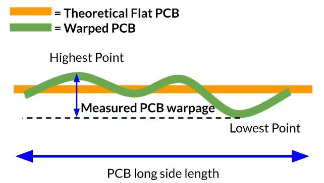
Stress during fabrication, such as thermal expansion and contraction, imbalanced copper distribution, and improper handling, can lead to warpage.
Utilize tools like feeler gauges, height gauges, contour gauges, optical profilometers, and Finite Element Method (FEM) simulations to accurately measure PCB warpage.
Effective design practices using OrCAD X, such as symmetrical component placement and proper copper distribution, combined with precise fabrication controls, can significantly reduce the risk of PCB warpage.


