Low dielectric loss characteristics (tan δ) and low resistance conductors, low electrical loss, suitable for high-frequency applications
Due to our unique manufacturing technology, the size and characteristics of each production batch and within each batch vary little
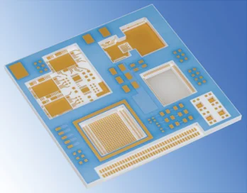
High-density wiring is achieved by improving stacking alignment accuracy
Precise control of substrate thickness and cavity shape
Resistance, inductance, and capacitance functions are built into the substrate and package

