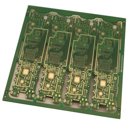
When designing high-speed PCBs, the layer stack-up plays a crucial role in ensuring signal integrity, minimizing crosstalk, and achieving optimal electromagnetic compatibility (EMC). For a standard six-layer board with a thickness of 1.6mm, selecting the right structure can significantly impact performance. Below is an analysis of common six-layer board structures and their suitability for high-speed designs
High-speed PCB design is crucial in fields like communication, computing, and graphics/image processing. Engineers in these areas often employ unique strategies tailored to their industry’s specific requirements. Below, we explore different approaches and key considerations for high-speed PCB design.
When designing high-speed PCBs, process variations and other factors can significantly impact actual impedance. Automated design tools may not always detect these subtleties, making proactive, defensive design essential. Here’s how to address common challenges in high-speed PCB design.
Before explaining the inspection work after PCB wiring is completed, we will first introduce three special PCB routing techniques. The routing of PCB LAYOUT will be explained from three aspects: right-angle routing, differential routing, and serpentine routing

