With the rise of high-speed DSPs (Digital Signal Processors) and peripherals, managing Electromagnetic Interference (EMI) has become a crucial aspect of design. In the past, issues of emission and interference were broadly referred to as EMI or RFI (Radio Frequency Interference). Today, these are part of a more nuanced area: Electromagnetic Compatibility (EMC), which encompasses both emission control and system immunity.
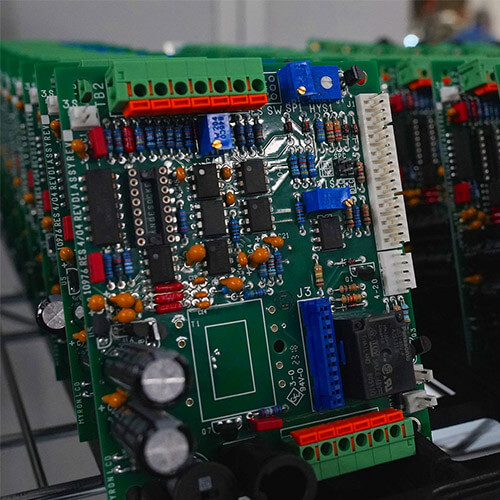
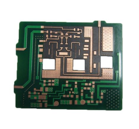
PCBs are critical in electronic devices, ensuring electrical connections between components. With increasing circuit density, proper PCB design techniques are essential to ensure reliability and reduce interference.
Printed circuit boards (PCBs) remain the backbone of electronic assembly across various systems. Even with perfectly designed schematics, poor PCB design can significantly compromise reliability. For instance, closely spaced thin parallel lines on a PCB can cause signal waveform delays and reflected noise at transmission line terminals. This guide outlines essential considerations for designing reliable PCBs.
Whether the signal quality will be affected depends on the method of adding test points and how fast the signal is. Basically, the additional test points (without using the existing vias (via or DIP pins) as test points) may be added to the line or a short line may be pulled out from the line. The former is equivalent to adding a very small capacitor to the line, and the latter is an additional branch

