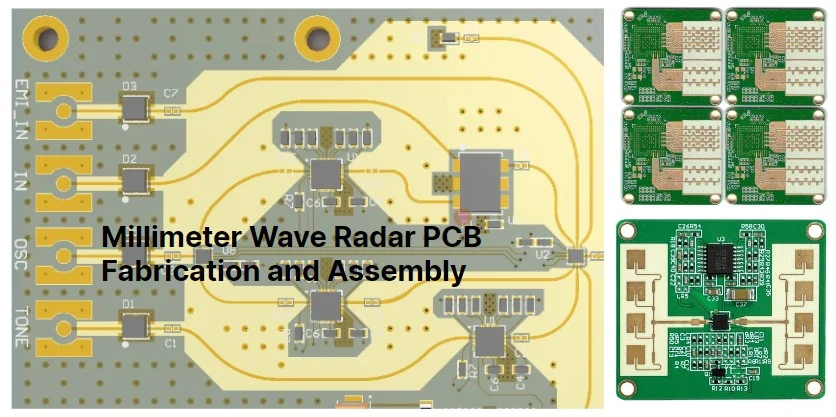
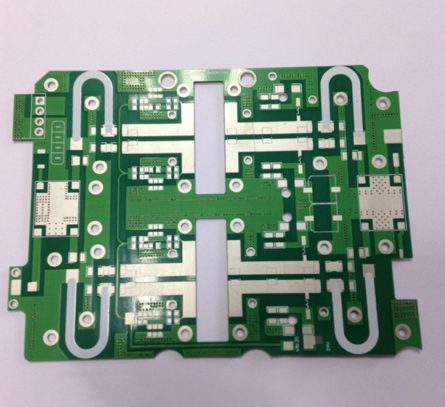
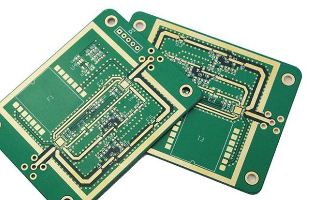
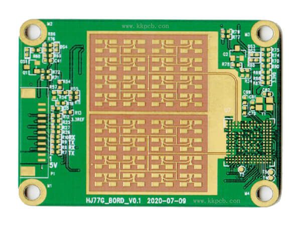
PCB Processing The precise dimensions required for millimeter-wave circuits demand well-controlled PCB processing techniques to produce circuits with consistently excellent performance. Variations in copper plating thickness and final surface treatment on the conductor surface can impact the performance of millimeter-wave circuits. To ensure the successful fabrication of high-performance millimeter-wave circuits, both of these processes must […]
Striplines are transmission lines embedded within a dielectric medium and are widely used in high-frequency circuits for their excellent signal integrity and predictable impedance. Broadside and edgewise striplines are two common configurations, differing in how the signal and ground planes are arranged. Understanding the design equations is crucial for impedance control and circuit optimization.
Printed Circuit Board (PCB) warpage refers to the phenomenon that the PCB plane bends or deforms due to various reasons during the manufacturing, storage or use of the PCB. This deformation may be local or overall, and is usually manifested as the PCB no longer remaining flat.
Addressing power supply noise interference in PCB design involves a systematic approach to layout optimization, filtering, and grounding. By understanding the root causes of power supply noise and applying the countermeasures outlined above, designers can significantly enhance circuit performance and reliability. A clean power supply, well-isolated signal paths, and proper filtering are key to achieving a noise-resilient PCB.
When applied correctly, copper coating offers more benefits than drawbacks, providing improved performance, noise reduction, and thermal management for PCBs. However, to achieve the best results, it’s crucial to carefully consider the design, including grounding, copper areas, and the specific requirements of high-frequency or low-frequency circuits. By paying attention to these details, designers can optimize the copper coating for better overall performance.
Grounding is a critical aspect of PCB design, particularly in mixed-signal environments where digital and analog circuits coexist. Proper grounding ensures stable performance, minimizes noise, and improves the reliability of the overall circuit. Below are key insights and guidelines to address grounding challenges effectively.
Often, products come without a circuit schematic, making it challenging to understand the PCB’s functionality and design principles. When faced with such a situation, follow these steps to reverse-engineer and restore the circuit diagram. This guide provides detailed instructions for accurately translating a physical PCB back into a schematic diagram.
PCB design translates electrical schematics into a functional product, and its quality directly impacts production efficiency and product reliability. For beginners, mastering PCB layout can be challenging despite familiarity with design software, and common issues often arise. Here, seasoned engineers from KKPCB share their PCB layout insights to help avoid these pitfalls and inspire best practices.
In today’s fast-developing electronic age, PCB printed circuit boards are the heart of electronic products, and their design and manufacturing technologies are constantly improving, especially in the field of high-frequency circuits. High-frequency circuit design is not only related to the performance stability of the product, but also directly affects signal integrity and electromagnetic compatibility (EMC).


