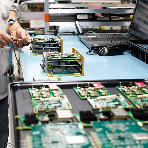
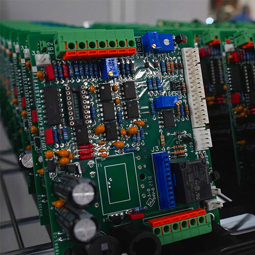
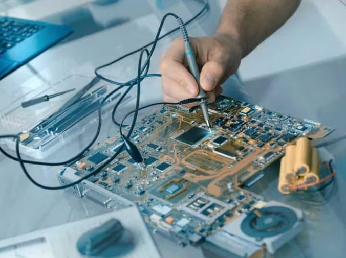
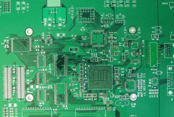
Troubleshooting printed circuit boards (PCBs) can be a daunting task, but with a systematic approach, it becomes manageable and efficient. This guide provides a step-by-step process to identify faulty components on PCBs, along with methods tailored to specific component types and advanced techniques for batch inspection.
PCB (Printed Circuit Board) substrate materials are the backbone of a PCB assembly, providing the necessary foundation for copper tracks and electronic components. The choice of PCB material plays a critical role in determining the performance, durability, and overall reliability of the PCB. These materials can be resin-based, fiberglass-based, epoxy-glass, metal-based, or flame-retardant, and they are selected based on the specific requirements of the PCB design and its application.
Staggered vias are a crucial element in the world of printed circuit board (PCB) design, especially for high-density interconnect (HDI) boards. But what exactly are they? Why are they important? Let’s take a deep dive into staggered vias and their benefits
HDI boards represent the forefront of PCB technology, enabling smaller, more efficient electronic devices while meeting the demands of modern consumer electronics and telecommunications.
HDI board is the abbreviation of High Density Inverter. It is a kind of (technology) for producing printed circuit boards. It is a circuit board with relatively high line distribution density using micro blind buried hole technology. HDI board is a compact product designed for small-capacity users. It adopts modular parallel design. One module has a capacity of 1000VA (height 1U), natural cooling, and can be directly placed in a 19″ rack. Up to 6 modules can be connected in parallel. This product adopts full digital signal process control (DSP) technology and multiple patented technologies. It has full range of load adaptability and strong short-term overload capacity, and can ignore the load power factor and peak factor.
In fact, there is no clear definition of HDI high-density manufacturing method, but generally there is a big difference between HDI and non-HDI. First of all, the aperture used in the circuit carrier made of HDI must be less than or equal to 6mil (1/1,000 inch), and the ring diameter of the hole ring must be ≦10mil, and the layout density of the line contacts must be greater than 130 points per square inch, and the line spacing of the signal line must be less than 3mil.
With HDI boards, you can affix more components on both sides of the bare PCB, allowing you to get more functionality in a smaller space and expand the overall functionality of your device. HDI technology enables you to add functionality while reducing the size and weight of your product.


