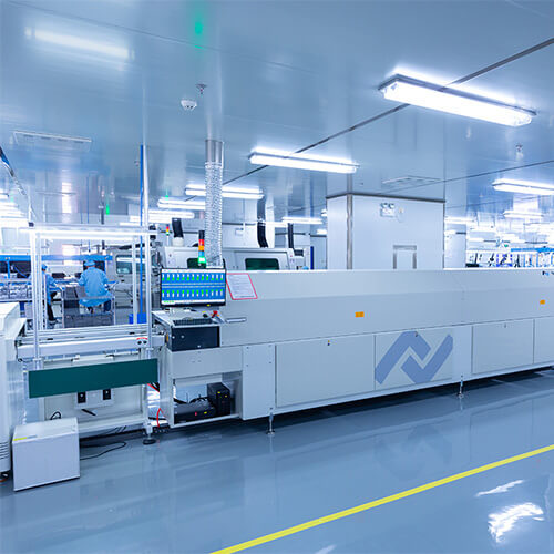
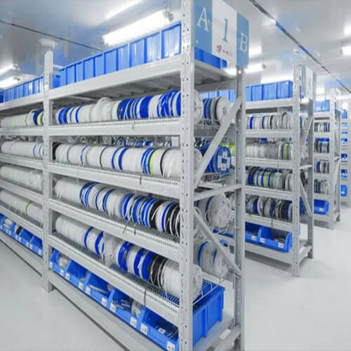
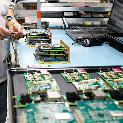
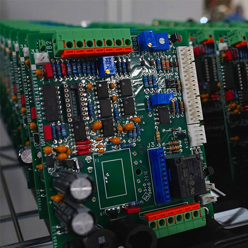
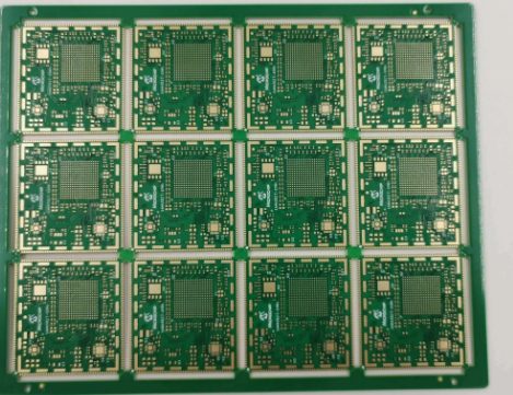
The manufacturing of HDI PCBs began in the late 1980s. With the successive production of PCBs, the first HDI production began in 1984. Since then, designers and manufacturers have been looking for ways to pack more components in a smaller area. HDI boards are designed and manufactured to comply with IPC-2315 and IPC-2226 standards.
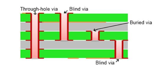
Vias are the copper-plated holes in the PCB that allows the layers to connect. The standard via is called a through-hole via, but there are several disadvantages to using through-hole vias in Surface Mount Technology (SMT). For this reason, we often use a blind via or buried via instead. A blind or buried via can be processed in a wide range of different measures, including plugged copper mask via, a plugged solder mask via, plated via or staggered via

