


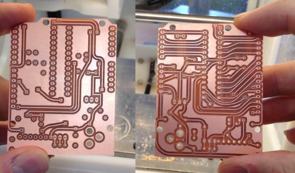
Designing double-sided PCBs requires careful planning to ensure efficient assembly, high yields, and reliable solder joints. Solder paste application and stencil design play a critical role in achieving these goals. This article explores key considerations for solder paste and stencil design, focusing on double-sided PCBs, component orientation, and advanced techniques for fine-pitch devices.
Electrostatic Discharge (ESD) can damage sensitive components such as MOSFETs, CMOS gates, and PN junctions, leading to issues like gate damage, short circuits, and even melted wiring. This guide offers practical strategies to design PCBs that effectively prevent ESD from harming the circuit.
Rigid PCBs are inherently versatile and are suitable for a variety of configurations from single to multi-layer. With KKPCB’s design for manufacturability and engineering services, you can find a rigid PCB that matches your size, material, and build specifications.