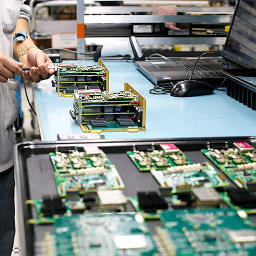
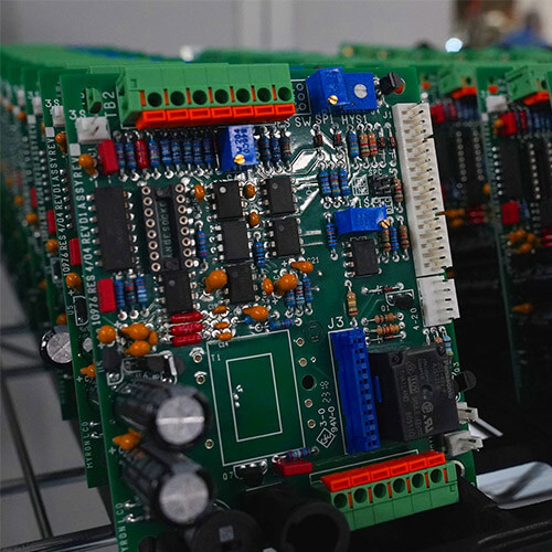
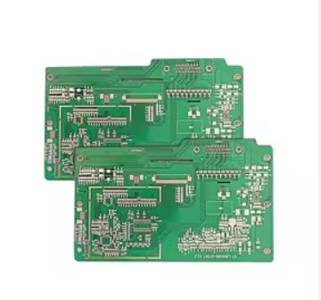
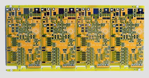
A Double-Sided PCB (also known as a Double-Layer PCB) is a type of printed circuit board where both sides of the substrate are used for placing electronic components and conductive copper traces. Unlike single-sided PCBs, which have a copper layer on only one side, double-sided PCBs feature conductive layers on both sides of the board, connected via plated-through holes (PTH), allowing circuits to connect between the top and bottom layers.
Single-sided and double-sided PCBs serve different purposes based on complexity and application needs. Single-sided PCBs are cost-effective and ideal for simpler designs, while double-sided PCBs provide flexibility and higher circuit density for advanced devices.
Printed circuit boards (PCBs) are the core of most electronics today, determining basic functions through combinations of components and wiring mechanisms. Most PCBs of the past were relatively simple and limited by manufacturing techniques, while today’s PCBs are much more complex. From advanced flexible options to odd-shaped varieties, PCBs are much more varied in nowadays’ world of electronics

