


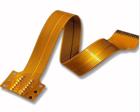
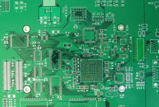
Printed Circuit Boards (PCBs) are the backbone of electronic devices, connecting components seamlessly for reliable functionality. Among these, Flexible LED PCBs have gained prominence due to their adaptability, reduced size, and cost-effectiveness compared to rigid PCBs. They are widely used across industries like consumer electronics, automotive, and aerospace
Circuit boards play a key role in making sure electronic products work properly. They provide structural support and link all the electrical parts together. Whether it’s in smartphones, laptops, or household devices, none could operate without a PCB
By adhering to these guidelines, engineers can ensure their PCB designs are manufacturable and optimized for high-quality production. These precautions and design considerations help reduce production errors, improve yield, and ensure the integrity of the final product.
By following these guidelines—such as optimizing trace width, minimizing via use, and ensuring proper documentation for manufacturing—you can significantly improve the performance, reliability, and manufacturability of your PCB designs.
HDI board is the abbreviation of High Density Inverter. It is a kind of (technology) for producing printed circuit boards. It is a circuit board with relatively high line distribution density using micro blind buried hole technology. HDI board is a compact product designed for small-capacity users. It adopts modular parallel design. One module has a capacity of 1000VA (height 1U), natural cooling, and can be directly placed in a 19″ rack. Up to 6 modules can be connected in parallel. This product adopts full digital signal process control (DSP) technology and multiple patented technologies. It has full range of load adaptability and strong short-term overload capacity, and can ignore the load power factor and peak factor.
In fact, there is no clear definition of HDI high-density manufacturing method, but generally there is a big difference between HDI and non-HDI. First of all, the aperture used in the circuit carrier made of HDI must be less than or equal to 6mil (1/1,000 inch), and the ring diameter of the hole ring must be ≦10mil, and the layout density of the line contacts must be greater than 130 points per square inch, and the line spacing of the signal line must be less than 3mil.