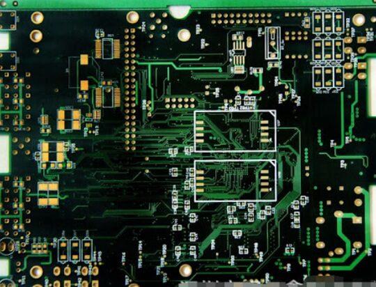
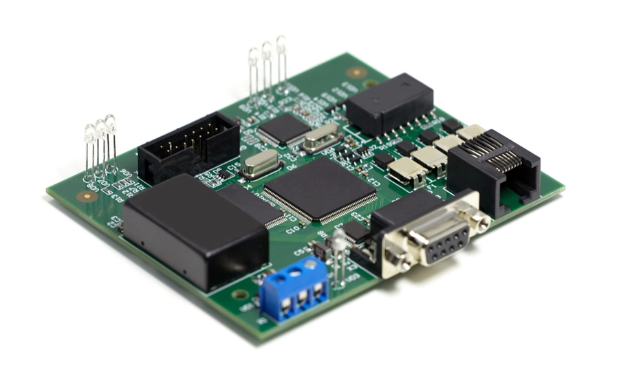
Following these practical tips for high-frequency PCB design helps in optimizing interconnections within the board. Techniques such as using 45° transmission lines, precision etching, and non-leaded components will significantly enhance circuit performance. Familiarizing yourself with these methods makes designs like back-copper coplanar microstrip layouts both economical and efficient.
Generally, multilayer circuit boards are designed with large amounts of copper foil as grounding devices. Sometimes, the Vcc layer is also designed with large amounts of copper foil. When these large amounts of copper foil cannot be evenly distributed on the same multilayer circuit board, it will cause problems with uneven heat absorption and heat dissipation rates. The multilayer circuit board will naturally expand and contract when heated and contract when cooled. If the expansion and contraction cannot be achieved at the same time, different ground stresses will be caused and the board will deform. At this time, if the temperature of the board has reached the limit of the Tg value, the board will gradually soften and cause deformation
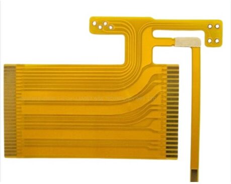
As the demand for even more compact electronics grows, so does the need for ultra-thin flex PCBs. PCBs are essential to the development of compact electronics for mobile, implantable and other small devices.
Key Takeaways
Defining two major concepts of board design and production: class and build.
An overview of the layout department’s responsibilities: library part generation as well as placement and routing.
Stepping more granularly through each task from schematic/design document reception to manufacturing files.

