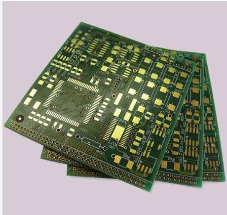
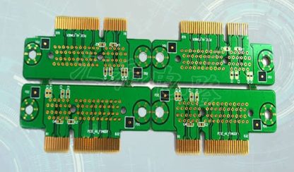
Excellent layer stacking is the key to ensure bypass and decoupling of the power bus, minimize transient voltage on the power layer or ground layer, and shield the electromagnetic field of the signal and power supply.
This article starts with the most basic PCB layout and discusses the role and design techniques of PCB layer stacking in controlling EMI radiation


