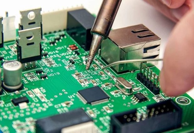
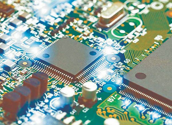
Standard PCB Thickness and Optimization
When designing a printed circuit board (PCB), engineers often focus on ensuring the correct impedance structures and electrical performance of the board. However, the physical characteristics, such as PCB thickness, are equally important and can significantly impact the cost, manufacturability, and performance of the final product. While standard PCB thicknesses are widely used, they are more of a convention than a strict requirement, offering designers an opportunity for optimization, especially in high-volume production.
Should I Use a Standard PCB Thickness?
The decision to use a standard PCB thickness depends on the specific requirements of your design. Here’s a breakdown of when to consider standard thicknesses and when to explore alternatives:
| Scenario | Use Standard Thickness? |
|---|---|
| When using a standard board edge connector. | Yes |
| When enclosure mounting or system requirements dictate this thickness. | Yes |
| Applications where reducing weight (e.g., aerospace) or vibrational susceptibility is key. | No |
| High-volume production lots to save on material costs. | Maybe |
| Besides the extra material cost, manufacturers generally have more experience working with standard thicknesses. | Yes |
Standard PCB Thicknesses Summarized
The most common PCB thickness is 1.57 mm (0.062 inches), which has become an industry standard due to its versatility and ease of manufacturing. Other common thicknesses include:
- 31 mils (0.031 inches)
- 62 mils (0.062 inches)
- 93 mils (0.093 inches)
- 125 mils (0.125 inches)
Tolerance Standards
- For boards with a thickness of 31 mils and above, the acceptable tolerance is typically ±10%.
- For boards with a thickness less than 31 mils, the tolerance is usually ±0.003 inches.
Copper Thickness and Its Impact
Copper thickness is another critical factor in PCB design, measured in ounces per square foot. Common copper weights include:
- 1 oz
- 2 oz
- 3 oz
Thicker copper layers can handle higher currents and improve heat dissipation, but they also increase the overall thickness of the PCB. For high-power applications, copper weights can go up to 6 oz, requiring adjustments to the base material to maintain mechanical stability.
Tolerance and Industry Standards
PCB thickness tolerance is crucial for ensuring proper fit and electrical performance. Industry standards like IPC-2221 provide guidelines for selecting thickness based on factors such as layer count, copper weight, and thermal considerations. Adhering to these standards ensures consistent manufacturing and compatibility with electronic components.
Design Determines Thickness
While standard thicknesses are convenient, design requirements should always take precedence. Reputable manufacturers will work with designers to meet specific thickness requirements, provided they are within reasonable limits. However, extreme thicknesses can increase costs and complicate manufacturing due to yield issues.
Key Considerations:
- Excess Thickness: Raises material costs and complicates manufacturing processes optimized for standard thicknesses.
- Extremely Thin Boards: May face production challenges and reduced mechanical stability.
- Dielectric Properties: Substrate thickness affects impedance and signal integrity.
- Weight and Vibration: Thinner boards are preferred in aerospace and high-vibration environments.
Determining an Appropriate Board Thickness
To determine the optimal PCB thickness, designers should consider the following factors:
1. General Circuit Density
- The conflicting demands of product miniaturization and functionality (e.g., power, EMI, and signal integrity) shape the stackup.
- Begin by assigning footprints to the BOM line items and importing the design into the board viewing environment to gauge placement and routing density.
2. Board-Edge Connectors
- Mating boards to other systems may require specific thicknesses for edge connectors.
- Collaborate with engineers and procurement to ensure design consistency and cost-effectiveness.
3. Enclosure Design
- System-level integration impacts board thickness, especially in wearables and small electronics.
- Early communication between engineering, design, and manufacturing teams is essential to set DFM design rules and minimize revisions.
While standard PCB thicknesses offer manufacturing consistency and cost savings, designers should not overlook the potential for optimization. By carefully considering factors such as circuit density, enclosure requirements, and material properties, engineers can determine the most appropriate thickness for their specific application. Collaboration with manufacturers and adherence to industry standards like IPC-2221 will ensure reliable and cost-effective PCB designs.
KKPCB provides global customers with one-stop services from PCB layout, prototype PCB proofing, PCB manufacturing, PCBA processing (including SMT and DIP), PCBA testing, PCBA product assembly and outbound packaging. You could provide a Gerber file or BOM list to us, we will offer the finished PCB products or PCB assembly which are satisfied with you.