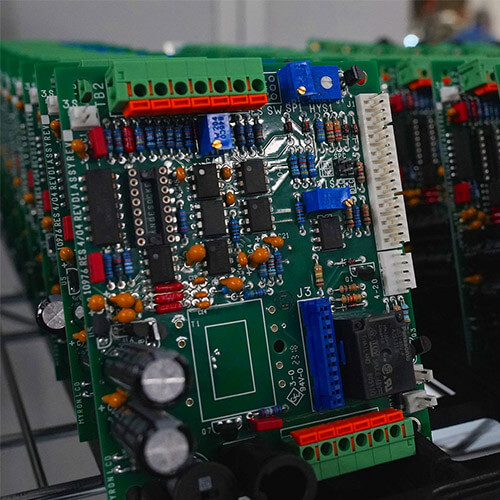
Staggered Vias in PCB Design: Benefits & Manufacturing
Staggered vias are a crucial element in the world of printed circuit board (PCB) design, especially for high-density interconnect (HDI) boards. But what exactly are they? Why are they important? Let’s take a deep dive into staggered vias and their benefits.
What Are Staggered Vias?
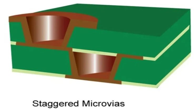
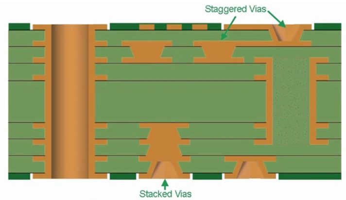
Staggered vias are tiny holes drilled at an offset across different layers of a PCB. These vias connect the layers of the circuit board, allowing signals to flow between them. Unlike traditional vias that go straight down in a vertical line, staggered vias are positioned slightly apart, usually in a diagonal or staggered arrangement.
Comparison to Stacked Vias
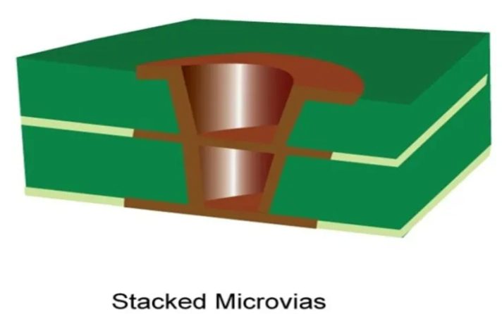
Staggered vias differ from stacked vias in both their design and performance. While stacked vias are drilled vertically aligned one on top of the other, creating a direct path through all layers of the PCB, staggered vias are offset from each other.
This offset helps in better signal routing and reduces the risk of interference, making staggered vias a more effective choice for high-frequency applications where signal integrity is critical.
Importance of Staggered Vias in HDI Boards
Space Efficiency
When designing HDI boards, space is everything. These boards are known for their compact size and high functionality. Staggered vias help optimize available space by allowing for better trace routing.
Also Read: What is PCB Routing?
Since they don’t stack directly on top of each other, they create more flexible pathways for signals, letting designers fit more functionality into a smaller area. This is especially important in industries like smartphones or wearables, where every inch counts.
Enhancing Signal Integrity
One of the biggest benefits of staggered vias is their ability to enhance signal integrity. When vias are too close together, such as in stacked via designs, they can cause signal crosstalk or electromagnetic interference (EMI), leading to degraded performance.
The offset nature of staggered vias reduces this risk by spreading the vias out and minimizing their interaction. This means less signal loss and more reliable performance, especially in high-speed applications like 5G networks or high-frequency circuits.
Thermal Management
Another crucial advantage of staggered vias is their thermal management capabilities. When vias are stacked, they can concentrate heat in one area of the board, causing thermal stress.
This heat can damage components or affect their performance over time. With staggered vias, the heat is spread out more evenly, helping to avoid hot spots and improve the overall thermal stability of the board.
This is particularly important in high-performance devices that generate a lot of heat, like gaming consoles or high-power electronics.
Advantages of Staggered Vias
Improved Routing Density
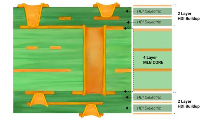
One of the primary advantages of staggered vias is their ability to increase routing density. In PCB design, space is precious, especially for high-density interconnect (HDI) boards. Staggered vias allow for more signal traces to be routed in the same area without crowding the board.
This enables more compact designs, making it possible to add more functionality to devices like smartphones, wearables, and medical gadgets without compromising performance. The optimized routing also leaves more room for components, which is critical in high-tech industries.
Reliability
Staggered vias offer better signal integrity, ensuring that your signals remain strong and clear. In high-speed circuits, stacked vias can cause issues like signal degradation or crosstalk due to their proximity to each other.
With staggered vias, the offset placement reduces interference, keeping the signals clean and reliable even at high frequencies.
This makes staggered vias a go-to choice for industries where performance and reliability are non-negotiable, such as telecommunications or automotive electronics.
Mechanical Stability
Staggered vias help reduce mechanical and thermal stress in your PCB. With stacked vias, the concentration of vias in a small area can lead to stress points in the board, especially when exposed to thermal cycles or physical shocks.
By distributing the vias more evenly, staggered vias spread out the stress, improving the overall mechanical stability of the board. This is essential for electronics used in harsh environments, like military or automotive applications, where durability is a must.
Design Flexibility
Another significant benefit of staggered vias is the design flexibility they provide. These vias allow for more intricate circuit designs without sacrificing performance.
Designers can use staggered vias to create complex layouts while still ensuring optimal signal integrity and thermal management.
Whether you’re designing for consumer electronics or medical devices, staggered vias provide the freedom to innovate and push the limits of what’s possible in compact, high-performance boards.
Manufacturing of Staggered Vias
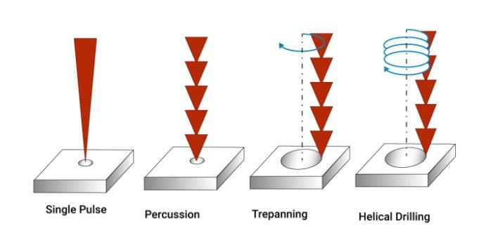
Laser Drilling Process
The creation of staggered vias often involves the laser drilling process, which allows manufacturers to achieve high precision and accuracy when creating microvias. Laser drilling is capable of producing very small holes with minimal tolerance, essential for the tight spaces found in HDI boards.
Unlike traditional mechanical drilling, which may not offer the required precision for such tiny vias, laser technology ensures that vias are drilled with the exact offset needed to achieve the desired staggered pattern.
This results in a more reliable connection between PCB layers, improving signal integrity and overall board performance.
Cost and Space Considerations
While staggered vias offer many benefits, they do come with some manufacturing challenges. The laser drilling process is more expensive than conventional drilling, which can increase production costs.
Additionally, creating staggered vias requires more board space than stacked vias because the vias must be placed at an offset rather than directly on top of each other. This can lead to larger board designs or increased complexity when fitting the vias into limited space.
Despite these challenges, many companies find the benefits of staggered vias—such as enhanced signal integrity and thermal stability—outweigh the additional cost.
For high-end applications where performance is critical, the investment in staggered vias often proves worthwhile, especially for industries like consumer electronics, automotive, and telecommunications, where compact and high-performing boards are essential.
Applications of Staggered Vias
Consumer Electronics
In consumer electronics like smartphones, tablets, and wearables, space is limited, and performance is key. Staggered vias help pack more functionality into compact designs while ensuring signal integrity and thermal management. This is critical for smooth device performance and energy efficiency.
Telecommunications
For telecommunications systems, such as 5G networks and fiber optics, staggered vias improve signal quality and reduce electromagnetic interference (EMI). By enabling high-speed, reliable data transmission, they help ensure that communication systems operate without disruptions.
Automotive and Medical Devices
In automotive and medical devices, reliability and performance are essential. Staggered vias allow for compact PCBs that maintain signal integrity and manage heat efficiently, ensuring these devices can withstand extreme conditions and function optimally in demanding environments.
FAQs About Staggered Vias
What is the difference between staggered vias and stacked vias?
The main difference lies in the alignment. Staggered vias are drilled at an offset across layers, while stacked vias are drilled directly on top of each other. Staggered vias provide better signal quality and reliability in high-performance designs, especially in HDI boards.
How does the manufacturing process for staggered vias work?
The manufacturing of staggered vias typically involves precision laser drilling, which allows for high accuracy in creating microvias. This process ensures the vias are placed at an offset, optimizing space and maintaining the performance of the PCB, though it can increase production costs.
Are staggered vias more expensive than stacked vias?
Yes, staggered vias are typically more expensive than stacked vias due to the precision drilling required. Laser drilling is more costly than conventional drilling, and the additional board space needed for staggered vias can further increase manufacturing costs.
In which industries are staggered vias commonly used?
Staggered vias are commonly used in industries where high-speed, compact PCB designs are essential. These include consumer electronics (smartphones, wearables), telecommunications (5G, fiber optics), and automotive and medical devices where reliability and performance are critical.
What challenges come with using staggered vias?
The primary challenges with staggered vias are space limitations and increased costs. The offset placement requires more space, which may impact component density on the PCB. Additionally, laser drilling and manufacturing add to the cost compared to other via types like stacked vias.
Staggered vias offer numerous benefits for high-performance, compact PCB designs, especially in industries like consumer electronics, telecommunications, and automotive.
Their ability to improve signal integrity, thermal management, and mechanical stability makes them a preferred choice for modern applications.
However, the challenges of space limitations and higher manufacturing costs should be carefully considered during the design process.

